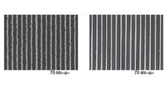
Miniature processors may hold more transistors working at reduced power requirements, but their manufacturing process is extremely intricate, and many of the produced semiconductors end up as trash because of tiny flaws in their surface.
However, the Princeton University researchers came up with an innovative method to melt away the defects in the lines, dots and other shapes etched on the semiconductor's surface. The new process could allow manufacturers to improve their yields, thus saving important sums of money in the fabrication process.
"We are able to achieve a precision and improvement far beyond what was previously thought achievable", said electrical engineer Stephen Chou, the Joseph C. Elgin Professor of Engineering, at the Princeton University.
Since semiconductors run at peak performance when they are shaped in the right proportions, eliminating the rough edges and other defects would dramatically improve the voltage fluctuations and leaks. "These chip defects pose serious roadblocks to future advances in many industries", Chou continued.
The method is called Self-Perfection by Liquefaction (SPEL) and is based on melting the structures on a chip, then guiding the resulting material in the optimal shapes. When using this process, lines are becoming straighter and dots get a perfectly round shape, thanks to the surface tension forces acting in the molten material.
"What we propose instead is a paradigm shift: rather than struggle to improve fabrication methods, we could simply fix the defects after fabrication", claimed Chou. "And fixing the defects could be automatic - a process of self-perfection", he continued.
Direct heat sources however, would destroy not only the imperfections but also the semiconductor itself. Chou came up with the idea of using the light pulse from an excimer laser (mostly used in eye surgery), as it can focus all the heat in a thin layer of material.
The researchers plan to implement their process in 8-inch silicon wafers and some semiconductor manufacturers are already interested in licensing the technology.

 14 DAY TRIAL //