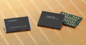
It looks like, disaster or no disaster, the semiconductor industry is going forward, with Toshiba now announcing that it too has advanced to a better, 2xnm process, at least for its newest collection of MLC NAND Flash memory.
Both DRAM and NAND, and the semiconductor segment as a whole, are expected to actually flourish this year.
For the former, analysts have already had their say, more than once actually, with the consensus being that things are looking up.
Ironically, the disaster that hit Japan on March 11 ended up having a positive effect of sorts in this area.
NAND Flash memory chips should see some good evolution as well, especially with the 2xnm processes kicking off.
Speaking of more advanced processes, Toshiba issued a press release to announce that it began using the 24nm.
To be more precise, the company developed 24nm-based SmartNAND embedded MLC (multi-level cell) NAND Flash memory chips with ECC (error correction code).
Available capacities are 4 GB, 8 GB, 16 GB, 32 GB and 64 GB, all of them being intended for such things as media players, digital TVs, set-top boxes and even tablets.
“Toshiba's new SmartNAND will provide our customers a smoother design experience into 24nm generation and beyond,” noted Scott Nelson, vice president, Memory Business Unit, Toshiba America Electronic Components, Inc.
“By enabling the system designer to directly manage the NAND using a standard or custom host NAND controller, while leaving the function of error correction within the NAND package, SmartNAND results in faster time to market, access to leading geometries and potentially lowers design costs when compared to conventional NAND flash implementations with external ECC.”
Some of the newcomers will start shipping as early as this month, while others could take as long as August to arrive. Either way, more information is available here.

 14 DAY TRIAL //