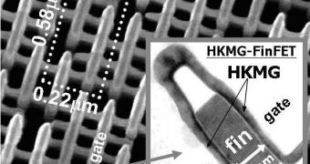
Toshiba Corporation, IBM and Advanced Micro Devices revealed yesterday the joint development of a Static Random Access Memory (SRAM) cell, which is said to feature an area of only 0.128 square micrometers (μm2). The SRAM cell announced by the three companies uses fin-shaped Field Effect Transistors (FinFETs) and is the smallest functional such part in the world.
The new cell has been developed using a high-k/metal gate (HKMG) material and is expected to provide advantages over planar-FET cells for future technology generations. Most systems-level, large-scale integrated circuits, like microprocessors, include SRAM cells as circuit components, and the shrinking of SRAM cells offers means of developing smaller, faster and more power efficient processors. The technology was unveiled on December 16, at the 2008 International Electron Devices Meeting in San Francisco, California, in a technical paper.
Usually, the reduction of transistor size on SRAM cells when conventional planar transistors are used is made by IC manufacturers through doping more impurities into the device area so as to adjust properties. Undesirable variability is created through this process, and the SRAM stability is deteriorated. The 22nm technology node and beyond see this as a critical issue. On the other hand, the use of FinFETs, vertical transistors that have fin-shaped undoped silicon channels, becomes an alternative that can allow the reduction of SRAM cell's size with diminished characteristic variation.
The FinFET SRAM cell fabricated by the three using HKMG is a highly scaled part, the smallest nonplanar-FET SRAM cell ever achieved. Having only 0.128μm2, the cell is about 50 percent smaller than the 0.274μm2 nonplanar-FET cell previously announced. The process has been optimized by the developing team that worked on the depositing and removing materials side, while including HKMG from vertical surfaces of the non-planar FinFET structure.
The research team also revealed having made investigations on stochastic variation of FinFET properties within the highly scaled SRAM cells, while also going for smaller cell size to simulated SRAM cell variations. According to them, the FinFETs without channel doping were able to improve transistor characteristic variability by more than 28 percent. They added that the FinFET SRAM cell of 0.063μm2 area (about the cell scaling for the 22nm node) was able to deliver a significant advantage in stable operation when compared to the planar-FET SRAM cell at the same size.
FinFETs turn into an attractive transistor structure for SRAMs in the 22nm node and beyond as a result of the successful development of highly scaled FinFET SRAM cells with HKMG achieved by the three companies. More powerful practical devices are now a step closer through the new technology.

 14 DAY TRIAL //