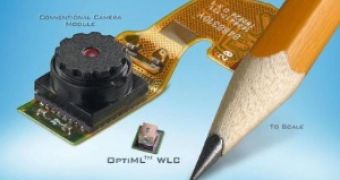
Tessera announced a new technology, called OptiML WLC (or OptiuL WLC) that allows cameras to be manufactured at the wafer level, resulting in a reduced size and bill-of-materials cost of camera modules found in mobile phones and other potable devices.
Using OptiML WLC technology, thousands of lenses are manufactured simultaneously on a wafer, and then bonded at the wafer level. The bonded lens wafers are then diced into individual lens modules, and each lens module is mounted on top of a packaged image sensor. Because common materials are used to build the lenses, the camera modules can be mounted directly onto the phone board using the same process used to assemble other electronics. This leads to cost savings of up to 30% for the optical component of the camera module.
OptiML WLC technology also reduces the size of the camera to a minimum, delivering up to 50% size reductions over conventional camera modules. For fixed focus applications, traditionally used for VGA to 2 megapixel resolution camera phones, OptiML WLC eliminates the need for manual focus adjustment of the cameras' optical elements. For 2 megapixel resolution and above, advanced auto focus and digital optical zoom can be integrated into the OptiML WLC solution using Eyesquad technology, without the use of moving parts. This provides enhanced camera functionality and reliability at lower costs and smaller form factors.
"We believe utilizing a wafer-level camera manufacturing technology is the most viable path to overcoming the challenges facing the industry today," said Bruce McWilliams, Tessera's Chairman, President and CEO. "With our acquisitions of Shellcase, Digital Optics and Eyesquad, we have assembled what we believe to be the strongest portfolio of camera optic technologies in the marketplace. For nearly two decades, Tessera has pioneered technologies that have resulted in smaller, better performing electronic products. We are continuing in that tradition with today's announcement, and we believe our OptiML wafer level camera technology represents a significant leap forward in the development of highly integrated, lower cost optics for consumer and other electronics."

 14 DAY TRIAL //