 14 DAY TRIAL //
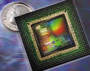
 Taiwan Semiconductor Manufacturing Company (TSMC) is proud to announce the first functional 65nm embedded DRAM products. TSMC's 65nm embedded DRAM process delivers a higher bandwidth as well as lower power consumption in a nearly 50% smaller cell and macro size than previous high density memory modules.
The higher bandwidth of the new 65nm eDRAM modules is recommended for game console, high-end networking devices and server/multimedia CPUs. Featuring a smaller manufacturing process, the new memories consume less active and stand-by power than what the market offers today, while it also eliminates the need to power up I/O appliances. In addition, the improved eDRAM's flexibility supports all the latest small factor designs by allowing the inclusion of both logic and memory functions on a single chip. This leads to a better board design, enhancing systems reliability altogether.
TSMC's new eDRAM design features extended power management options for low power applications including sleep mode, partial power cut-off and on-chip temperature compensation. The new 65nm manufacturing process for eDRAM memories implies the use of up to 10 metal layers using copper low-k interconnect and nickel silicide transistor interconnect methods. Thanks to a reduced cell size (less than ? of previous SRAM sizes), the eDRAM chips come in macro densities ranging from 4Mbits to 256Mbits.
"We've talked to customers and understand their needs. TSMC firmly believes that this new embedded DRAM process and IP are well suited for the demands created by the convergence of the wireless, consumer and communications devices. The results will be multi-functional computing platform that will spawn the next generation of innovation," said Jason Chen, vice president of corporate development, TSMC.
All new 65nm memory chips specifications are supported by TSMC's Design Support Ecosystem program featuring DFM-compliant 65nm products and services. Moreover, TSMC's Reference Flow 7.0 design methodology and SRAM compiler libraries have been updated to support the 65nm process.