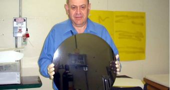
Although analysts are skeptical, TSMC, one of the major supporters of the transition towards 450mm wafers for integrated circuit fabrication, has just announced that the company will build the first such product pilot line in 2013-2014, mass production to begin in 2015-2016.
The announcement was made during a conference call with financial analysts by Morris Change, TSMC's chief executive officer and chairman.
"Our first 450mm pilot line is planned at our Fab12 Phase VI, starting with 20nm technology. The timing of pilot line will be around 2013, 2014.
Our first 450mm production line is planned in around 2015, 2016," stated the company's CEO.
As X-bit Labs reports, this bold claim suggests that the company has pretty much finalized its plans regarding the new production facility.
However, analysts aren't as optimist as TSMC is, as one of the major hurdles that has to be overcome by the transition to 450mm wafers is the equipment suppliers reluctance to develop the tools needed, as they still haven't managed to get the profit they anticipated from the switch to 300mm.
“The equipment suppliers did not realize an acceptable ROI on their R&D investment in 300mm tools and they are hesitant to fund development of 450mm wafer capable tools,” said Gus Richard, an analyst with Piper Jaffray, just last week.
Right now, Intel is the only company, outside of TSMC, that has firm plans to open a 450mm wafer facility, as the Santa Clara-based company is getting ready to start 450mm research and development at its D1X lab sometime in 2013.
The European Commission is also interested in the benefits that a 450mm semiconductor prototype foundry cold bring to Europe.
Taiwan Semiconductor Manufacturing Company fabricates chips for a large number of companies, including AMD, Qualcomm, Altera, Broadcom, Conexant, Intel, Marvell, Nvidia, and VIA, and is the world's largest dedicated independent semiconductor foundry.

 14 DAY TRIAL //