14 DAY TRIAL //
 If you have been with us during the first two episodes of taking apart Sony's Google TV then you most certainly know that we still haven't discovered what makes this Android powered TV tick, but all that is going to change today as the guys from Nikkei Electronics Teardown Squad have finally reached that all important third and final board said to hide an Atom CE4100 chip.
However, before going forward with this, I suggest you to also take a look at the first and second part of this teardown, in case that you somehow missed one or even both of them.
But moving back to the matter at hand, using pretty much the same process as that needed for taking down the TV side heatsink (you must remember that crazy method that added more solder to the board in order to remove the heatsink) the Teardown Squad managed to take a look at what powers this thing.
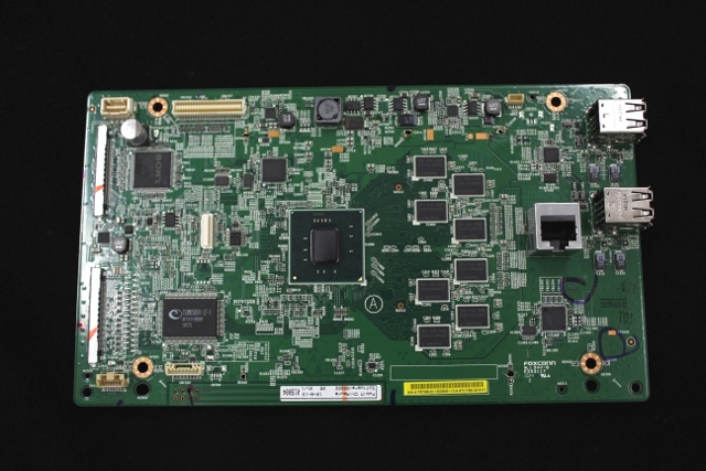
As everyone suspected, behind the heatsink is an Intel Atom CE4100 processor that is specially designed to be used in consumer electronic products, such as IP enabled HDTVs.
Since this is actually a System-on-Chip (SoC) design, the processors also houses a display processor, graphics processor, video display controller, transport processor, a dedicated security processor and general I/O including SATA-300 and USB 2.0 controller on the same die as the CPU.
Featuring a powerful video decoding graphics processor, Intel says this chip can decode two 1080p MPEG2 or H.264 video streams at the same time, more than enough to handle Sony's TV requirements.
Apart from the CE4100 SoC, the squad also found 1GB of DDR3 RAM built by Samsung Semiconductor, the back of the card housing two flash memory chips and a flash drive controller (for what basically forms an SSD), connected to the Atom SoC via a SATA interface.
Finally, I will leave you with the full image set describing the TV's teardown, from episode 1 to 3 in the right order.