14 DAY TRIAL //
 Soon after our arrival in Japan, the guys over at Sony informed us that we would get a chance to visit their high-tech facility in the Nagano Prefecture. Located a couple of hours away from Tokyo, this place was said to incorporate the essence of VAIO design, bringing all steps of a new notebook design under the same roof. Basically, we were told that we would visit the place where some of Sony's most valuable notebook PCs were designed and manufactured.
Obviously, this was one opportunity that we couldn't miss out, especially since our technology senses began tinkling the first time we set foot in Japan. In addition, having a chance to go into the lion's lair, or so to speak, left us wondering whether we could catch a glimpse of some unreleased products that Sony might be cooking up, here at its high-end facility. With that in mind, we took our fully-charged cameras and laptops and waited patiently for the bus to take us to the place where some of your favorite VAIOs are born.
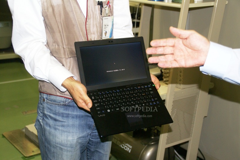
Some time after our departure from Tokyo, we reached Nagano TEC, in the Azumino City, Nagano Prefecture. After arriving, we got a briefing on the company's strategy, concerning the Nagano facility, but also on some of the latest Vaio products, manufactured here. We shall talk more about our briefing at a later time, so please feel free to come back for an update.
Unfortunately, during the briefing, we were told, much to our disappointment, that we couldn't bring our cameras along with us, but a designated photographer would take shots of the things we indicated, thus providing Sony with a better management of what information goes out of the company. Obviously, no other means of visually recording the different parts of the Nagano factory were allowed, only a Sony employee that we persistently stressed out with our requests.
With this minor setback, we put on the slippers and jacket that we were supposed to wear inside the factory and went on for a tour of the building where the magic happens.
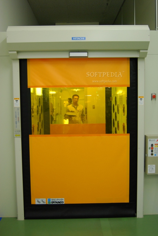
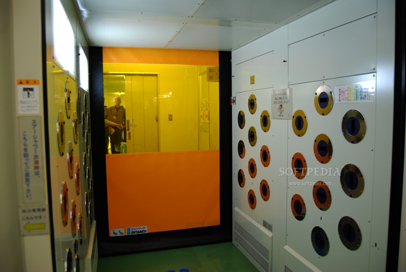
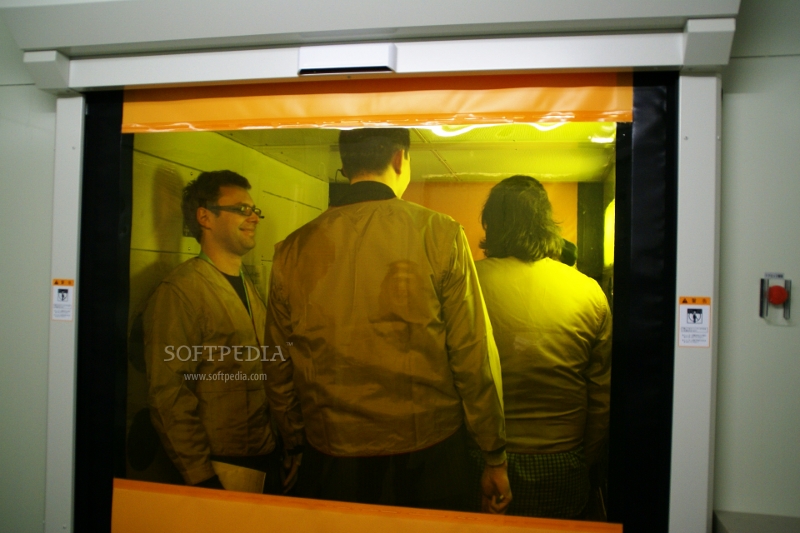
Before we were able to set foot inside this temple of technology, we had to go through a special chamber that is designed to blow the dust or other small particles away from our clothes, since we would be interacting with some of the smallest parts inside a notebook computer. And when I say small, I say considerably smaller than a grain of rice. After letting the chamber clean us up, we were finally inside the Sony Nagano factory.
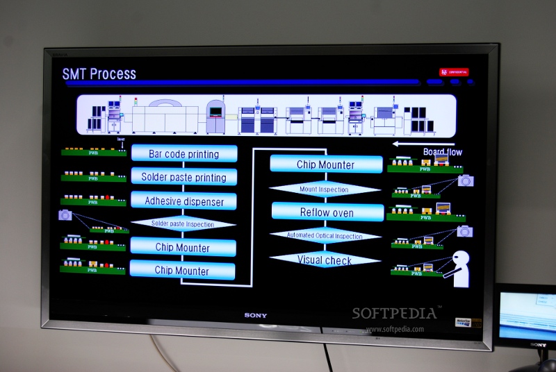
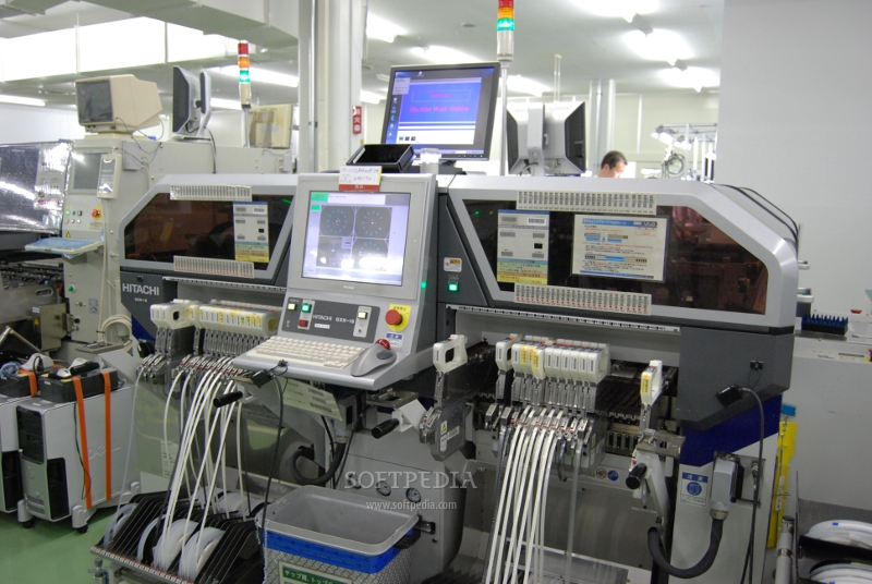
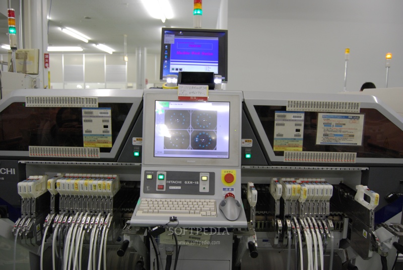
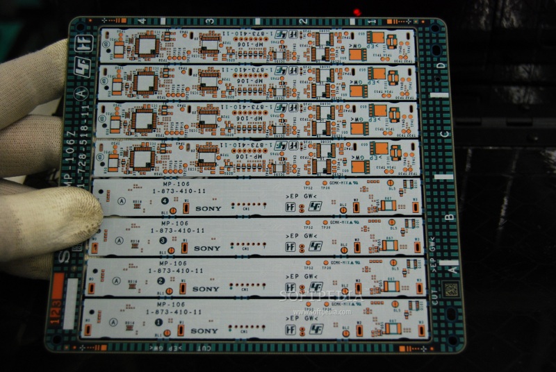
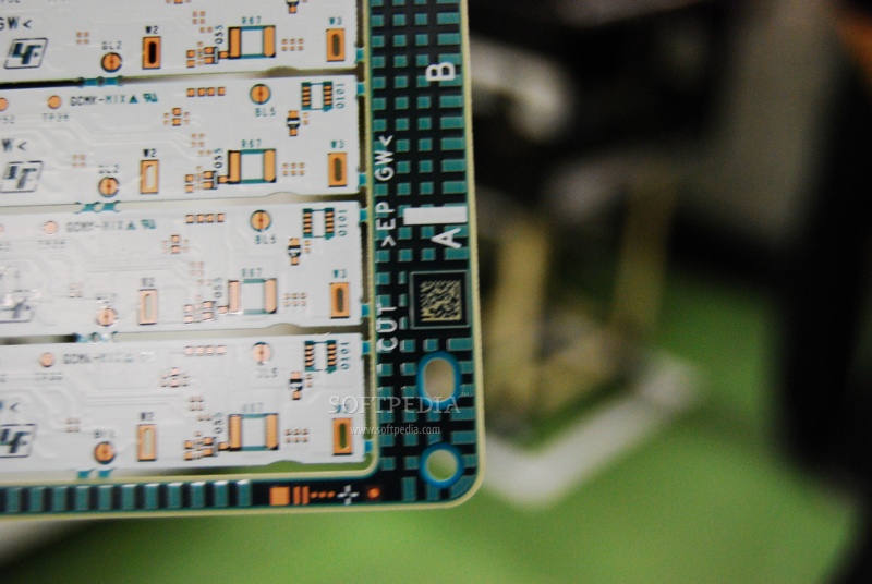
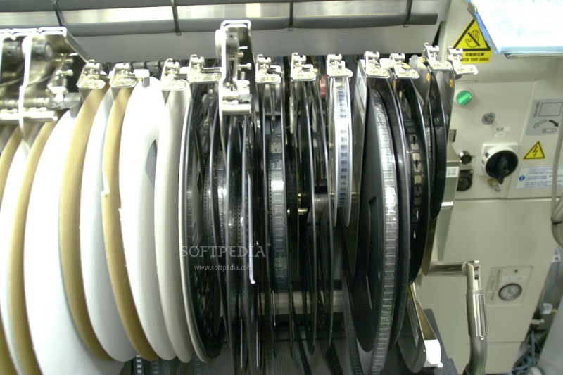
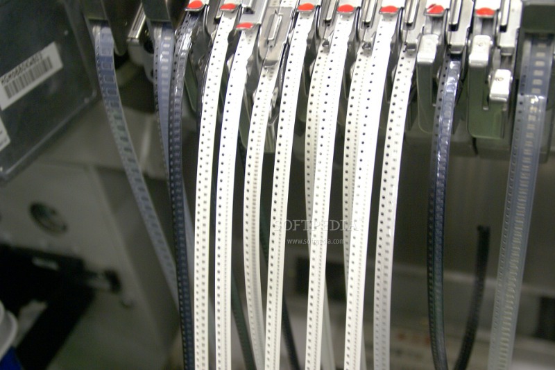
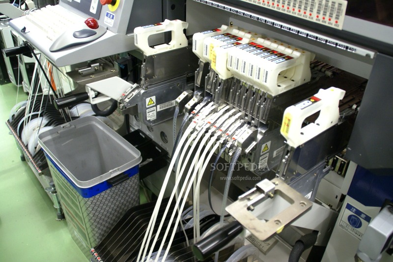
The tour started off with an assembly line where a series of connected machines was used to put different chips on different PCBs. This is where we saw that small chip we talked about earlier, smaller than a grain of rice. Mind our enthusiasm for a series of machines that were meant to solder chips on a PCB, the process itself is impressive. In fact, Sony provided us with a very clear explanation of the entire route of a PCB from start to the final inspection. These machines were loaded with film-like rolls that featured small chips on them, ready to be put to good use on a specific PCB.
While there are a lot of chambers inside the Nagano facility, we were only shown a select few, but enough to get some perspective on what the Vaio notebook design process consists of. After the chip assembly chamber, we were directed to a room where they test Vaio laptops for their toughness factor. Basically, here is where they are going to stress out the laptop so that it could perform within the necessary parameters throughout its entire lifetime. We are talking about drop tests, dust tests and tests of extreme weather conditions.
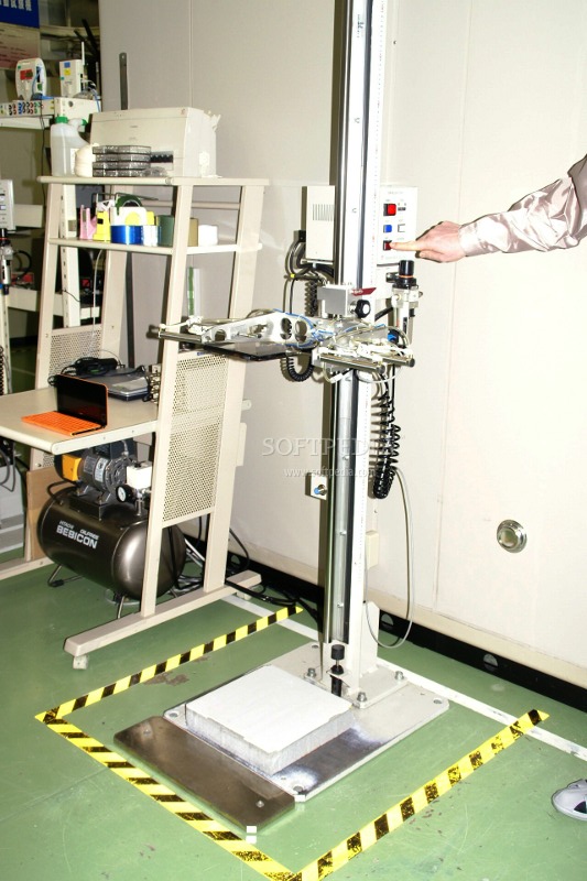
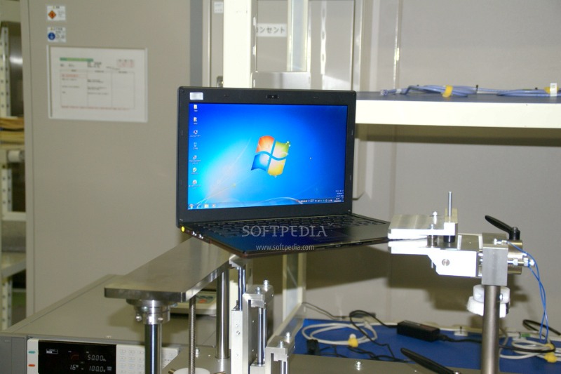
As you can see in the pictures below, the sensitive Vaio X series is treated with some considerable punishment, something that isn't likely to happen under normal conditions. Nevertheless, a test is a test and the fellows over at Nagano SNT wanted us to see that, even after a drop of 90cm, the fragile Vaio X can still pack a punch. This means that, in the unlikely event of a laptop to fall from 90cm, the operating system and the entire system will still work, pretty much the same way it did before the unexpected drop. Obviously, this isn't something we recommend for the folks back home, as the drop test is performed under lab conditions, but it was interesting to see that in action.
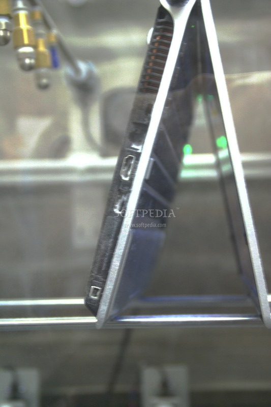
With the Vaio X, the Sony engineers had another challenge to tackle. They wanted to make the lightest and thinnest notebook around, but clearly not the most fragile one. On that note, there's this machine that was designed to stress just one corner of the laptop, a test that was inspired from real-life conditions. There are some users that will pick up the laptop from one of the corners, with the lid open. In this case, with the Vaio X, there's a chance that the product could break, but only if the user handles it in a more brutal matter. As we saw in the facility, despite its reduced form factor, the Vaio X isn't as vulnerable as one would imagine.
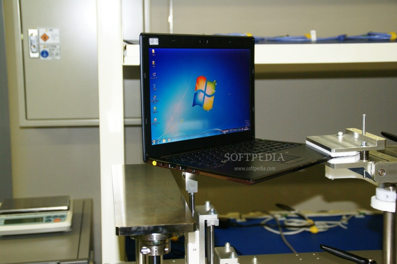
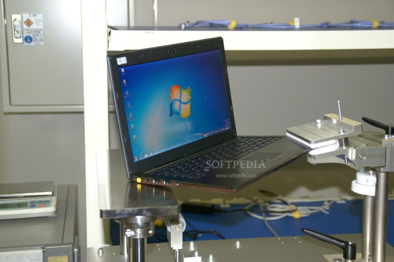
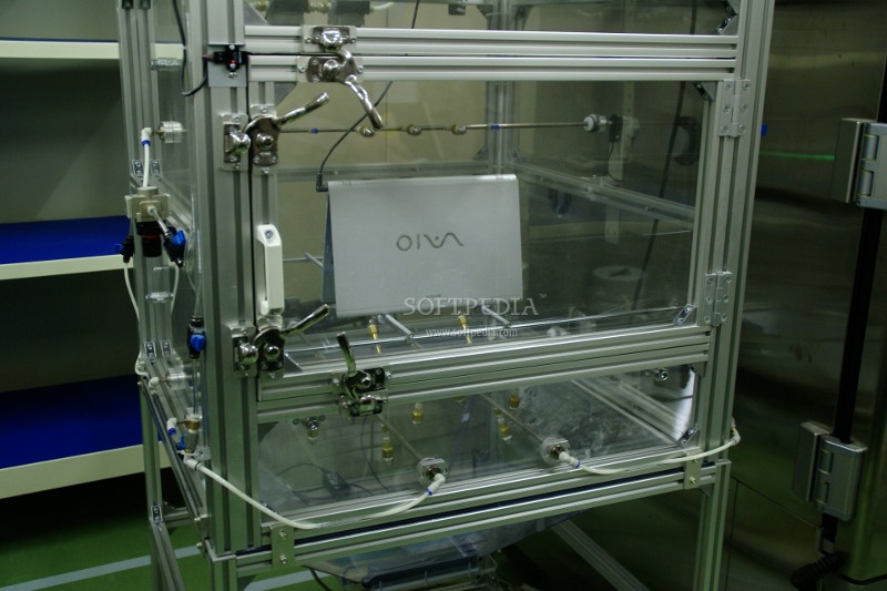
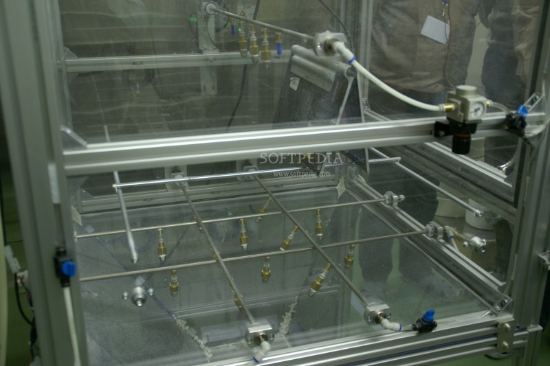
Just before we left this test room, we were presented with a small chamber where they were testing the laptop's ability to function in dusty environments. In this transparent chamber, a Vaio was sitting around waiting silently, unaware of the treatment it's going to receive after a small button would be pressed. That button was enthusiastically pressed by one of the journalists and in no time particles of dust were being thrown and blown into the laptop, simulating some very extreme working conditions. That's basically what Sony wanted, saying that they were looking to test it under the most extreme conditions.
We will have more on our extensive tour of the Nagano factory in an upcoming article, which will include some of the more interesting parts of the tour. So stick around as we'll make our way towards the final part of our visit to Japan.