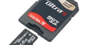
The two companies have signed a memorandum through which they begin the collaboration in the development, manufacturing and selling process of NAND memory and NAND related products. In this new project, they are undertaking both companies will invest equal amounts of money.
O.C.Kwon, Senior Vice President of Hynix Semiconductor Inc., said, "We are very pleased to successfully conclude negotiations with SanDisk in a way that will benefit the customers and shareholders of both companies. With the patent cross license behind us, we are able to put aside distractions and turn our attention to a very promising relationship in the development of x4 technology. We look forward to building on this relationship to our companies' mutual benefit."
The NAND memory they are going to manufacture is based on x4 technology and it allows four times more information to be stored than on Single Layered Cells (SLCs) NAND and up to twice the storing capacity of Multi Layered Cells (MLCs). Both of these NAND memory types are currently used in flash drive manufacturing, from Pen Drives to memory cards for digital photo cameras.
Eli Harari, Chairman of the Board of Directors and CEO of SanDisk, said: "This cross license agreement resolves all IP issues between Hynix and SanDisk, and allows each company to focus on maximizing its opportunities. Hynix has done an outstanding job in NAND flash manufacturing in the past few years, and I look forward to cooperating with Hynix through the joint venture planned between our two companies."
Between the two types of NAND memory modules, the main differences are in the number of read/write cycles each allows and the speed at which they operate. SLC NAND is used for flash memory that requires speed and a long time of service, being able to sustain up to 1.000.000 read/write cycles.

 14 DAY TRIAL //