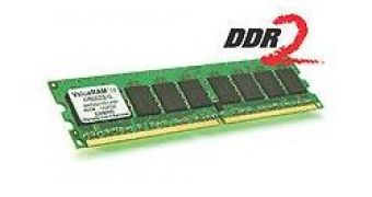
Samsung Electronics announced today that it successfully completed the development of the first 2Gb DDR2 random access memory chips that will be built using the more advanced 60 nanometer fabrication process and that the mass production is scheduled to start at the end of the year. The random access memory manufacturing industry is currently using the 80 nanometer fabrication process for the 2Gb DDR2 chips and Samsung will have a big advantage over the market as the new process comes with a series of important advantages both for the manufacturing company and for the end user.
The new fabrication process brings a sustained speed of 800 megabits per second, which means an improvement in performance by 20 percent when compared to the 80nm fabrication process. On the manufacturing company side, the new process will mean that the very same production lines will now be able to increase their output by 40 percent for 2Gb DDR2 memory chips, as the 60 nanometer process is based on a much finer technology. As the market trend is to move towards higher densities and bigger storage capabilities, in order to satisfy the demand for bigger and faster memory solutions, the new 60nm manufacturing process will simply double the storage capacity of existing memory solutions.
According to a press release from Samsung, the new high capacity and high performance memory modules will be well suited for ''applications in servers, workstations and notebook PCs where operating speed is a major concern''. The new 2Gb DDR2 random access memory device simply cuts in half the total number of components needed to build an 8GB memory module and the new solution also consumes 30 percent less power than a module built using 1Gb chips.
Samsung will build and ship four types of memories based on the new technology: 8GB fully-buffered, dual inline memory modules (FBDIMMs); 8GB registered, dual inline memory modules (RDIMMs); 4GB unbuffered, dual inline memory modules (UDIMMs); and 4GB small outline, dual inline memory modules (SODIMMs). As the mass production of 2Gb DDR2 chips is due to start by the end of the year, the manufacturing company will soon have a complete product line up based on the new 60nm fabrication process, with memory chips ranging in capacity between 512Mb and 2Gb. Gartner Dataquest, an industry and market research company, expects the total value of the 2Gb random access memory market value to top around $14 billion and it is also expected to reach around 47 percent of the total DRAM market by 2011.

 14 DAY TRIAL //