Samsung is the world's largest supplier of NAND Flash memory modules and in order to maintain its position, the company's constantly trying to improve on the design of its chips, besides trying to make the manufacturing processes more efficient. And yet another proof of Samsung's sustained efforts comes with the company's latest announcement, since the company has just announced that it has developed the world's first 64 Gigabit (Gb) multi level cell (MLC) NAND flash memory chip that uses 30-nanometer (nm)-class process technology.
This new flash memory device represents quite an important step forward in the adoption of higher-density flash storage solutions, since this new technology allows a maximum of 16 64Gb flash devices that can be combined to make a 128 Gigabyte (GB) memory card that can store 80 DVD resolution movies or 32,000 MP3 music files.
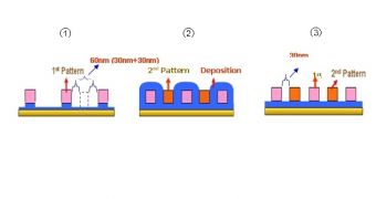
The new flash device was successfully developed through the use of a new manufacturing process called self-aligned double patterning technology (SaDPT). In SaDPT, the 1st pattern transfer is a wider-spaced circuit design of the target process technology, while the 2nd pattern transfer fills in the spaced area with a more closely designed pattern.
SaDPT represents a pivotal advancement beyond the charge trap flash (CTF) technology that Samsung developed for NAND flash last year when it introduced a new material (silicon nitride) and a new structural configuration. SaDPT resolves a critical bottleneck to forming sub-30nm circuitry by expanding the role that conventional lithography technology plays in the manufacturing process. Both Samsung's CTF-based NAND flash technology and SaDPT are expected to provide improvements in cost efficiency for next-generation nanometer-scale designs.
Samsung's SaDPT will employ existing photolithography equipment in 30nm-class production, which is expected to be commercialized beginning in 2009. By utilizing conventional photolithography equipment, Samsung can not only significantly speed up the process but also improve the cost efficiency of its manufacturing operations without additional facility investment.
Samsung also has developed a 32Gb single level cell (SLC) NAND flash chip based on the same technology applied to its 64Gb chip. The company expects to begin production of 30nm-class 64Gb flash devices in 2009 and the market prospects seem to be quite appealing since, according to Gartner Dataquest, the accumulated sales for 64Gb NAND flash and higher density devices could reach up to $20 billion in just three years.
We are just a few, but there are many of you, Softpedia users, out there. That's why we thought it would be a good idea to create an email address for you to help us a little in finding gadgets we missed. Interesting links are bound to be posted with recognition going mainly to those who submit. The address is  .
.

 14 DAY TRIAL //