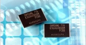
Semiconductor manufacturer Samsung Electronics has begun mass production for 16 gigabit (Gb) NAND flash. These modules are fabricated using the 51 nanometers (nm) process node and are expected to be produced with 60 percent more efficiency than the former 60nm manufacturing process.
These 16 gigabit memory modules are going to come in quite handy as they have multi-level cells (MLC) and are the building material for 16GB memory products, such as SD cards, or pendrives, or even as storage devices. By using the 51nm process node, the speeds that can be achieved by the memory chips are almost 80 percent faster than current 60nm-built products, allowing read speed of up to 30MB/s and write speeds of up to 8MB/s. By comparison to the faster single-level cell (SLC) based products manufactured on the 60nm process node, these modules reach very similar speeds, as those SLCs can read with up to 33MB/s and write with 13MB/s.
Memory modules such as these also feature a 4-bit error correcting code (ECC), but they have significant changes on the read/write pattern. In 60nm NAND flash memory you would find the basic information block, called a "page", to be in a 2 KiloByte (KB) page size, whereas in the new 51nm NAND flash memory products, the page size increased to 4KB.
Jim Elliott, director, flash marketing, Samsung Semiconductor said: "In rolling out the densest NAND flash in the world, we are throwing open the gates to a much wider playing field for flash-driven consumer electronics. To minimize production costs and improve performance, we have applied the finest process technology a 'half generation' ahead of the industry, which is introducing 55nm and higher."

 14 DAY TRIAL //