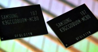
New memory chips are made quite often, and it looks like Samsung delivered on its status as semiconductor company by coming up with MLC NAND chips equipped with the DDR2 interface.
Since solid state drives, smartphones, tablets and other Flash-using electronics could always do with more speeds, Samsung figured it was time for another move.
As such, it came forth and delivered a certain sort of chips that are described as the first of their kind, being basically NAND Flash units designed with the Double Data Rate 2.0 interface, otherwise known as DDR2.
The chip has a capacity of 64 Gb and is built on the 20nm manufacturing process technology, while the interface gives it a high performance beyond not just SDR NAND, but also toggle DDR 1.0.
For those that want exact numbers, the maximum transfer rate of the newcomer is 400 Mbps, this being a threefold boost over DDR 1.0 (133 Mbps) and a tenfold one over the 40 Mbps of SDR NAND.
Thanks to these performance parameters, the chips will work best in conjunction with the USB 3.0 and SATA 6.0 Gbps interfaces.
To these advantages is added the fact that the smaller process allows for a productivity increase of about 50% over 20nm-class 32 GB toggle DDR 1.0 solutions and 100% over 30nm 32 Gb MLC NAND.
“With this 20nm-class, 64Gb, toggle DDR 2.0 NAND, Samsung is leading the market, which is evolving to fourth-generation smartphones and SATA 6Gbps SSDs,” said Wanhoon Hong, executive vice president, memory sales & marketing, Samsung Electronics.
“We will continue to aggressively develop the world's most advanced toggle DDR NAND flash solutions with higher performance and density, since we see them as vital to enabling a greater diversity of services for mobile phone users worldwide.”
It shouldn't be long before the 64 Gb DDR2 NAND starts to show up in real products.

 14 DAY TRIAL //