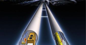
Scientists at the US Department of Energy's (DOE) Thomas Jefferson National Accelerator Facility have recently taken a huge step forward in advancing particle-accelerator technology when they have created the first US-built superconducting radiofrequency (SRF) niobium cavity. The new instrument was designed specifically to meet the specifications of the proposed International Linear Collider (ILC), whose exact building location has not yet been precisely determined.
The goal of the ILC is to allow its operators to study matter at very high levels of energy. It will work by colliding electrons and positrons together, and will have an initial energy capacity of 500 giga-electronvolts (GeV). An upgrade to 1,000 Gev is also possible, the structure's Technical Design Report also shows. The facility will be between 30 and 50 kilometers (19 to 31 miles) long, about ten times the size of the largest existing linear-particle physics experiment, the 50 GeV Stanford Linear Accelerator (SLAC).
“This is the first cavity built and processed in the US that exceeds the ILC gradient specification established by the ILC Global Design Effort,” the Global Design Effort (GDE) Cavity Group leader Rongli Geng, who is also a staff scientist at the Jefferson Lab, explains. In charge of actually constructing the SRF niobium cavity was Medford, NY-based Advanced Energy Systems, Inc. The structure was then processed, assembled in its final form, and eventually tested at the Jefferson Lab.
“We will follow this path of success and treat the next two cavities [similarly]. I anticipate favorable results will follow shortly and AES will soon be regarded as a high-quality source for ILC superconducting RF cavities,” Geng says. “It's always the partnership between labs and industry that makes benefits for both,” AES CEO and Director Tony Favale adds.
“It is a major ILC superconducting RF milestone and it is good news for JLab, for AES, for the Department of Energy and for Fermilab. We believe an improvement in cavity treatment for material property optimization specific to AES cavities may have been responsible for these remarkable results. This is the fruit of the new temperature-mapping and the optical-inspection tools we introduced into the process about a year ago under the guidance of ILC GDE project managers,” Geng concludes.

 14 DAY TRIAL //