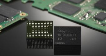
Multi-level cell NAND flash memory (MLC NAND for short) continues to be the most commonly used and affordable type of solid-state storage, and this must be why SK Hynix so diligently worked on advancing its manufacturing process.
The thing about semiconductors is that their performance and capacity depends on the type of manufacturing technology used to create them.
The width of the process, measured in nanometers, is what it all boils down to. The smaller the process, the better things get.
Well, that's an oversimplification, but an ultimately accurate one, more or less. SK Hynix has been proving it, time after time.
Case in point, SK Hynix has introduced the world's first 16nm NAND Flash chip, which also happens to be the highest-capacity NAND MLC chip ever made.
Which is to say, it has a storage size of 128 Gb, or 16 GB. All thanks to 16nm 64 Gb MLC processing technology.
SK Hynix had to solve a key issue here though, namely that of higher interference among cells the smaller the technology gets.
The Air-Gap technology was used, to overcome that interference, by building insulation shields with vacuum holes between circuits.
Previously, certain isolating substances were used for this, but at that level, it becomes too troublesome, if not impossible, to gain the same benefits.
SK Hynix intends to see the 16nm 16 GB NAND used in everything from memory cards to SSDs. Meanwhile, it will advance TLC (Triple Level Cell) and 3D NAND Flash too.
"After the Company developed and started to mass produce the industry's thinnest 16nm product then now prepared high density NAND Flash product portfolio thanks to the development of 16nm 128 Gb MLC," said Senior Vice President Jin Woong Kim, the head of Flash Tech Development.
"The Company plans to actively respond to our customers' demands with the NAND Flash products which have high reliability and endurance," he added.

 14 DAY TRIAL //