We have extremely powerful electronic computers these days and it's great, but scientists fear that we might not be so fortunate in the near future, as microchip minimization cannot go forever in order to supply the required computing power. Photonic crystals are just one of the solutions we could imply to create faster and faster computers. Photomic crystals are organized structures that have the capability of conducting light in a particular wavelength, while all other light frequencies are blocked from interfering with the correct functioning of system.
As early as the 1980s, researchers have been able to replicate a series of 2D and 3D optic crystals, but they proved to be extremely expensive to build in order to be used in the electronics industry. Now, the European Union-funded Photonic Hybrid Architectures based on Two- and Three- Dimensional Silicon Photonic Crystals, or PHAT, claims to have been able to create a photonic crystal that is much easier to fabricate, cheaper and ready to be integrated directly into silicon chips.
The properties of the photonic crystal are rather similar to that of layers of liquid, which present 'One-dimensional' structures. However, these properties are extended to two or even three dimensions in the case of the photonic crystals. For example, two-dimensional crystals can be used successfully as waveguides and filters for different wavelengths, while three-dimensional ones could even be able to trap light within their volume and function as an optical transistor.
The materials of choice in the electro-optical communication technology can be inexpensive substances such as gallium arsenide and indium phosphide semiconductors. On the other hand, integrating optical crystals into silicon chips is a totally different story, bringing extra complexities related to the size of the optical components which tend to be much larger than electronic components.
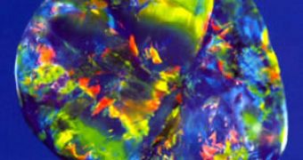
It may pass as much as two decades before photonic crystals become fully integrated into silicon chips. PHAT scientists argue that, by using combined 3D and 2D photonic crystals, all-optical computer chips could become as small as 10 to 100 times the size of the standard silicon processor. By using a specific construction technique, PHAT assembled artificial opals out of 250-900 nm in diameter silica beads only ten beads deep to create a 3D photonic crystal, but the refractive index of the material is so low that it cannot be used for practical applications.
Through the use of a chemical vapor deposition technique, a St. Petersburg company improved the refractive index of the 3D photonic crystal by filling the spaces between the spherical beads with silicon, only to totally remove the beads later on. The next step would be creating defects in the structure of the 3D photonic crystal, as it is created as a perfect crystal and has no functional role in its rough state. The last part of the fabrication process would most likely involve bringing together both 3D and 2D crystals.
The PHAT program reached its end nearly one year ago, and succeeded in creating the first 3D photonic crystal with waveguides.

 14 DAY TRIAL //