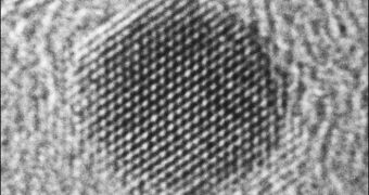
A new class of electronic memory technologies was developed by experts at the University of California in Berkeley (UCB), and the National Nano Device Laboratories, in Hsinchu, Taiwan. The technology can store and erase data 10 to 100 times faster than existing charge-storage memories.
This was made possible through the use of nanoscale dots (nanodots). Each of these structures is made up of billions of nanomagnets, whose polarity can be controlled. Changes in polarity are used to encode data, in the form of binary information (1s and 0s).
In the future, hard drives based on nanodots will have the ability to store hundreds of times more data than conventional devices in use today, e! Science News reports. For now however, researchers have to take things one step at a time.
The nanodots that the international collaboration created are just 3 nanometers across, and are made out of silicon. Each of these structures – behaving as an individual memory bit – is embedded in a layer of non-conducting material, the investigators report.
On top of this substrate, experts added a thin metallic layer, which they say acts like a metallic gate. The purpose of this membrane is to control the state of the newly-formed transistor – either on or off.
Details of how the nanodot-based memory technology was achieved are published in the latest issue of the esteemed journal Applied Physics Letters, which is edited by the American Institute of Physics.
“The metal-gate structure is a mainstream technology on the path toward nanoscale complementary metal-oxide-semiconductor (CMOS) memory technology,” explains study coauthor and NNDL research scientist, Jia-Min Shieh.
“Our system uses numerous, discrete silicon nanodots for charge storage and removal. These charges can enter (data write) and leave (data erase) the numerous discrete nanodots in a quick and simple way,” the expert goes on to say.
The polarity of the embedded nanodots is changed using ultra-short bursts of green laser light, which create temporary gates over the desired dots. This control method is extremely precise, the team says.
“The materials and the processes used for the devices are also compatible with current main-stream integrated circuit technologies. This technology not only meets the current CMOS process line, but can also be applied to other advanced-structure devices,” Shieh concludes.

 14 DAY TRIAL //