Currently available image sensors are still made much in the same way as any other silicon chip, through an expensive etching technique that creates tiny structures on the surface of the semiconductor. But by making the sensor out of a forest of nanowires grown from the bottom up, researchers argue that a new type of high-quality light sensing device can be built in square meter sheets at a time, with relatively low costs in comparison to silicon based sensors.
A prototype of such a device was recently created by Ali Javey and his team, of the University of California, Berkeley, who pioneered the technique. Nanowires are chemically grown on a surface and then printed onto another. "At the first stage, the nanowires are more-or-less standing up, like a bad hair day. But during the printing process, they effectively get combed," said Javey.
The printing surface can be made of a wide spectrum of materials, starting from silicon all the way to paper, but has to be prepared so that the nanowires are guided into predetermined locations. The nanowires themselves are made out of two compounds, cadmium selenide and silicon-coated germanium, the first having the role of converting light into electric charge while the second makes the base for a simple transistor in order to amplify the signal.
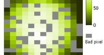
The prototype created at the University of California consists of a sensing device with 260 pixels, each of them being built out of five nanowires. "It's the largest integrated device to date based on nanowires. Imagine having a tape - just like your sticky tape - that you can grab and put on anywhere you want. This tape will have all the needed components to do the active sensing, translate the data, and transmit it wirelessly," Javey said about the new image sensor, at the same time pointing out that the device is flexible, reliable, can be easily scaled up and could be made into rolls of wireless tape a couple of meters across. Currently the research team in working on nanoscale batteries and other wireless components.
This is the first study to demonstrate that chemically grown nanowires from bottom up can be used in the assembly of electronic devices. "I really like what they have done here," said John Rogers of the University of Illinois at Urbana-Champaign.

 14 DAY TRIAL //