Researchers at the University of Florida announce the development of a new type of transistor that is made entirely out of carbon nanotubes (CNT). The innovation could be used to create an advanced generation of TV and computer screens, experts believe.
The CNT-based transistor could become the next big thing in TV technology, the research team explains. The devices consume considerably less electricity than conventional transistors, while at the same time maintaining a comparable clarity of detail and brightness, LiveScience reports.
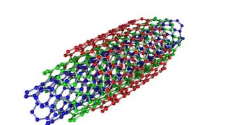
Carbon nanotubes are made out of individual carbon atoms, which are joined together in a hexagonal, honeycomb-like pattern. They can be grown in several flavors from different substrates, but can also be manufactured directly, by rolling a sheet of graphene into a tube.
This material has tremendous theoretical applications – in a wide array of scientific fields – which is exactly why experts are so interested in discovering more about its properties, which include improved electrical conductivity and tremendous strength.
One of the most interesting things about nanotube transistors is that they could be used to generate much larger displays, especially of the type manufactured using organic light-emitting diodes (OLED).
“Our device opens up a whole new realm of materials that could solve this size limitation problem” that OLED-based displays have, explains UF professor of physics Andrew Rinzler. The expert is also a coauthor of a new paper detailing the findings, which appears in the April 28 issue of Science.
“This is great work with very encouraging results, which can have significant impacts in future OLED displays,” comments expert Yang Yang. He describes the CNT-based transistors as “very smart,” but he was not a part of the team that conducted the new work.
The scientist holds an appointment as a professor of materials science and engineering at the University of California in Los Angeles (UCLA). He adds that the new devices will however have to undergo a process of miniaturization.
Pixels today have dimensions of around 200 by 300 micrometers, whereas the pixels produced with the carbon nanotube transistors are about 1 square millimeter. As soon as this issue is settled, the transistors can be moved towards large-scale production.

 14 DAY TRIAL //