Nanopillars are extremely small filaments of material, with sizes of just a few billionths of a millimeter. Growing them on polymer substrates has proven to be a very daunting task over the past decade, because science teams couldn't figure out how to individually separate them, and make them “grow” in the patterns modern applications demand. Now, the physical mechanism for this has been finally uncovered at the California Institute of Technology (Caltech).
With the new research, it may now become possible to grow the nanoscale pillars in potentially endless patterns, which may bring about a considerable boost in the industry. Caltech Professor of Applied Physics, Aeronautics, and Mechanical Engineering Sandra Troian has been the leader of the team that has managed to develop the new nanofluidic process. The innovation is described in the latest issue of the respected scientific journal Physical Review Letters.
Building large nanoarrays at high resolutions at this point relies heavily on conventional photolithographic patterning techniques, such as the ones used in the electronics industry today. These processes make use of ultraviolet light and harsh chemicals to etch various patterns on silicon substrates, which are the basis for a wide array of chips. Integrated circuits and microelectromechanical devices are two of the most common applications for these methods.
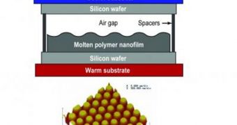
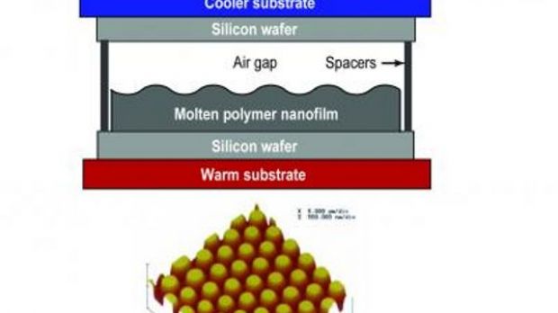
The production process is also what ultimately limits the performances of the devices, as the repeated chemical treatments cause a lot of surface roughness. “This process is also inherently two-dimensional, and thus three-dimensional structures must be patterned layer by layer,” Troian explains. Some time ago, a group of researchers discovered that, when inserting molten polymer nanofilms inside a slender gap separating two silicon wafers, nanopillars spontaneously formed. When the mix was chilled, self-assembled, evenly spaced, honeycomb-like structures solidified.
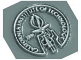
Troian's method relies on microfluidic applications. She explains, “You can see this effect very nicely if you move an ice cube in a figure eight beneath a metal sheet coated with a liquid like glycerol. The liquid wells up above the cube as it traces out the figure. You can draw your name in this way, and, presto! You have got yourself a new form of thermocapillary lithography!” She concludes, “We are shooting for nanostructures with specularly smooth surfaces – as smooth as you could ever make them – and 3-D shapes that are not easily attainable using conventional lithography.”

 14 DAY TRIAL //
