14 DAY TRIAL //
 Recently, NVIDIA has decided to speak about how closely it worked with TSMC on the Kepler GPUs, instead of both companies working separately.
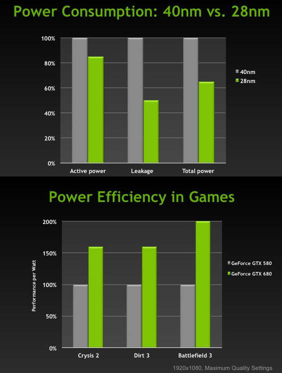
Seeing the energy efficiency benefits, not to mention the better state of the 28nm node compared to 40nm (yield/shipment-wise), the two are going to keep collaborating on future products too.
That is to say, both NVIDIA and TSMC will adjust their chip creation/manufacture processes as needed.
In fact, the blog post where NVIDIA explored all this closed with a brief mention that the Santa Clara, California-based company had already received the first version of an enhanced PQV (Product Qualification Vehicle) test chip for 20nm.
It will take some time before we know just what further enhancement to power efficiency and performance the world is in for. NVIDIA, of course, expects them to be significant, but we'll wait and see.