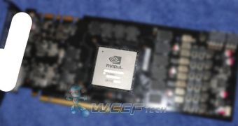
NVIDIA's fabled GeForce Titan graphics adapter has been getting mentioned in the news several times a week lately. Now, though, we at least have something to actually show, literally.
WCCFTech has posted an exclusive preview of the adapter's printed circuit board (PCB).
It is a very blurry image, and it might have been made so deliberately, since there isn't much of a justification for photos to be so hazy, not with how good cameras are these days.
At any rate, the picture shows two PCI Express power connectors (one 6-pin, one 8-pin), 12 memory chips, an 8+2+2 phase VRM (hard to tell) and an integrated heatspreader on the GPU.
The reverse side probably has an extra 12 memory chips, unless NVIDIA somehow found 4 Gb GDDR5 chips to use (unlikely).
There is a 4-pin fan connector too, implying that the cooler probably has a single spinner, though it will still take up two PCI slots.
2 SLI goldfingers can be seen as well, enabling quad-SLI support. It will take a huge mainboard to fit four dual-slot adapters, but it was done in the past.
That is all that we can see in the picture. The rest of the specs still have to be confirmed.
Then again, the GK110 has been used in the Tesla K20 supercomputer compute accelerators, so we know what it has to offer at least, though the clock speed, like the speed of the VRAM, is still under wraps.
The Kepler chip has 2,688 CUDA cores (a positively massive number), a memory interface of 384 bits, up to 3X performance-per-watt of Fermi (GF110) and 15 SMX units. The whitepaper found here has everything else of relevance.
Backed by 6 GB of GDDR5 VRAM (this being the standard amount, not an OEM choice), the processor will breeze through everything buyers will throw at it.

 14 DAY TRIAL //