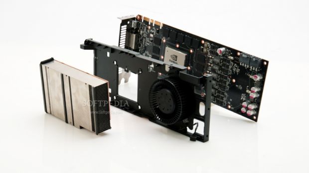
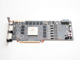
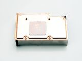
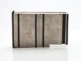
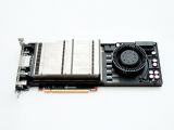
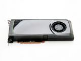
You've been reading a whole lotta things about NVIDIA's latest addition to the GTX family, the super-powerful, "world's fastest DirectX 11" GPU, namely the GeForce GTX 580, which has just swiftly taken up the flagship position in NVIDIA's lineup, but now, it's time for a rather different approach, one that involves a bit of...disassembling.
Courtesy of NVIDIA, we've been able to test the GTX 580 (albeit briefly), and although we'll present our conclusions regarding the board itself a little later, we've decided to offer you a bit of a sneak preview at what you should expect from it, at least as far as the the insides of the board are concerned.
First of all, we'll have to mention that taking the GTX 580 apart is a pretty difficult job, the very large number of tight screws making the whole process quite time-consuming.
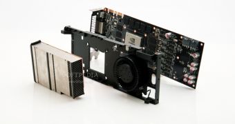
The first step was to remove the top protective case, which left us with a very interesting view of the fan, plus the vapor chamber cooling solution implemented by NVIDIA on their latest GPU.
However, we didnt' stop at that, and also removed the cooling block in order to reveal the board's "heart and sould", namely the GF110 graphics processing unit.
Putting the whole thing back together was a pretty easy task, all things considered, although we'll have to admit we required quite a decent amount of silicone paste in order to ensure an OK fit between the card and the cooling chamber.
 14 DAY TRIAL //