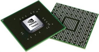
While the Tegra 2 SoC has been out in the open for quite some time now, Nvidia wasn't very forthcoming when it came to detailing the GPU architecture used inside this chip, the very first pieces of the puzzle just making their way onto the web.
Just as many other pieces of information regarding the Tegra 2, these too were disclosed by Fudzilla, the website stating that the SoC's GPU is capable of rendering 71 million triangles per second.
This makes the Tegra 2 SoC just a tad slower in the graphics department than the Power VR SGX 540 that is used in the Samsung Galaxy S smartphone as well as in a few other portable devices.
In order to achieve this level of performance, Fudzilla claims Nvidia went with a programmable pixel shader as well as with a programmable vertex and lightning engine, enabling Tegra 2 to push up to 1200 million pixels per second, in certain conditions.
Furthermore, Tegra's 2 GPU is also capable of Coverage Sampling Aliasing (CSAA), a technique first introduced in the GeForce 8 series of graphics cards.
Meant to reduce line ruggedness, this AA method uses Z, color, and coverage information to determine final pixel color, making the resulting image look crisp and sharp.
As far as connectivity options are concerned, the GPU supports HDMI 1.3 as well as analog VGA or LVDS, some implementations of the chip allowing for WSXGA+ (1680x050) resolution at 24-bit color.
A 1.3 HDMI output capable of 1080p video playback rounds the list, the GPU being fully capable of decoding Full HD video streams in various formats, including H.264, VC-1 and MPEG-4.
Although these are all the details available for now, Tegra 2 seems like a really powerful architecture that has more in common with graphics cards released a few years back than mobile GPUs.

 14 DAY TRIAL //