Computer chip manufacturers are well aware of the fact that measurement uncertainty is hampering the further miniaturization of the nanoscale components that go into electronics today. For these companies, a new study by American researchers may provide a breath of fresh air.
Investigators at the US National Institute of Standards and Technology (NIST) announce that they have recently completed a study on how to refine the measurement of objects at the nanoscale. The approach provides highly accurate data that could contribute to innovation in the field of electronics, they say.
The team says that multiple measuring instruments and statistical techniques are combined in this approach, which has already elicited a lot of interest from major computer chip manufacturers.
These companies have to deal with measuring millions and billions of tiny switches every single day. These nanoscale components can be so small that even the tiniest measurement uncertainty can have significant repercussions, hampering performances, and rendering research budgets unfruitful.
By using the NIST nanoscale measurement technique, it is now possible to accurately determine the size of structures less than a few dozen nanometers across, something that was impossible before.
It's very important to keep in mind that current miniaturization standards produce chip components so small that not even an optical microscope can make them out directly. The distance between transistors on a modern microprocessor is smaller than the distance between air molecules.
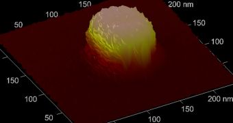
Thus far, techniques such as scatterometry (which analyzes light diffraction patterns from the target object) and atomic force microscopy (AFM) have been used to determine the size of nanostructures. Even with these slow and time-consuming approaches, uncertainty remains.
“Maybe scatterometry tells you the width of an object is 40 nanometers, but it's plus or minus three nanometers, a relatively large variance. Making things worse, the total uncertainty usually increases when measurement techniques are combined, making our vision even hazier,” Richard Silver says.
The NIST scientist says that a combination of scanning techniques and statistical analysis can provide more accurate data, a lot faster and cheaper than the methods used previously.
“In essence, if you've got a really small uncertainty in your AFM measurement but a big one in your optical measurements, the final uncertainty will end up even smaller than either of them,” Silver adds.
“IBM and GLOBALFOUNDRIES have already begun developing the technique since we first described it at a 2009 conference, and they are improving their measurements using this hybrid approach,” he concludes.

 14 DAY TRIAL //