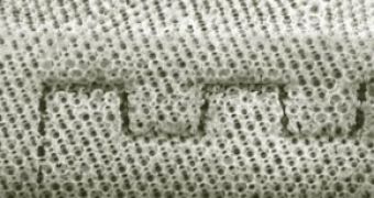
Invisibility cloaks and ultra-fast computers could one day be powered by such an exotic device, however, multiple problems need to be solved before these crystals become useful. Several metamaterials have been designed over the years, but the technological process involved in building them presents multiple technological difficulties, as most of it relies on creating a complex metal nanostructure, disabling the mass production possibility.
Furthermore, these photonic crystals, which use variations of the indices of refraction in the structure, present only partial invisibility properties for the light spectrum, as the material is transparent only to certain wavelengths in the light spectrum.
The new photonic crystal, developed at the University of Illinois, by Paul Braun, uses its optical properties in order to transmit optical signals through designated paths inside it, which could serve as a telecommunications medium, or as cavities for laser systems using low power ratios during the starting process. Until now, all the previously designed metamaterials presented only 2D waveguides, while the new device presents waveguide properties in all dimensions.
The basic building process of the new photonic crystal is extremely similar to that of making metamaterials and involves creating a semiconductor structure of colloid silica spheres, with diameters of 725 or 925 nanometers on a substrate, which has a crystal configuration similar to that of opal (a naturally occurring crystal that has a high-refractive silicon structure, which includes pockets of air with low-refracting properties).
After creating the silica sphere embedded in the substrate, the structure receives a monomer solution that is bonded together with the help of a laser, in order to create a polymer. After this, the whole structure is filled with silicon, and the silica spheres are extracted out of it, by washing it with an acid, which leaves the silicon structure behind.
The resulting silica based photonic crystal is transparent enough to light close to the infrared spectrum. While testing its light conducting capabilities, the developer of the 3D photonic crystal fired a light beam through a channel that presented two sharp bends, and discovered that light in the 1.48 micrometers wavelength was detected on the other side, corresponding to the bandgap of the material.

 14 DAY TRIAL //