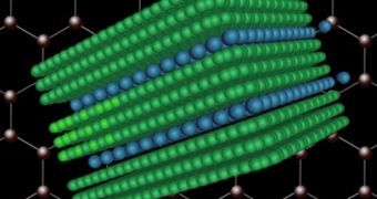
A group of investigators at the Massachusetts Institute of Technology (MIT) announces the creation of multi-layered graphene, a carbon compound that is believed to be silicon's replacement in electronics.
The material – the strongest in the world – has chemical and physical properties that are appealing to a variety of industries and applications, but thus far researchers have been unable to produce the 2D matrix in a way that allows it to have a band gap.
Without such a gap, it's impossible to use the one-atom-thick compound for any practical applications. MIT experts could not let the unique strength and the electrical and thermal conductivity go unused.
As such, they developed a way of producing graphene in double or triple layers. The experts say that this will help the material become usable for the production of revolutionary transistors, solar cells, computer chips and related electronic components.
Physicists at the Institute say that arranging the two or three layers in precisely the right configuration results in the creation of the long-sought-for band gap. This is an energy range that can be found between the energy levels where electrons can exist in any given material.
With the gaps obtained, and the multi-layered material produced in large amounts, the MIT team has basically eliminated two of the most obtrusive obstacles blocking the path of progress in this field.
“It’s a breakthrough in graphene technology,” explains the MIT Charles and Hilda Roddey associate professor of chemical engineering Michael Strano. He is also the author of a new paper describing the findings, which appears in this week's issue of the top journal Nature Nanotechnology.
Professor of chemical engineering Daniel Blankschtein, MIT graduate student Chih-Jen Shih and 10 other students and postdoctoral researchers were co-authors of the groundbreaking investigation.
According to the authors, the new material is “one of the most promising candidates for post-silicon nanoelectronics.” In the paper, they explain that the technique used to produce the material is a derivative of a method produced at MIT in the 1950s.
“Because this dispersion process can be very gentle, we end up with much larger flakes [than usual]. Graphene is a very fragile material, so it requires gentle processing,” Strano explains. Another method for obtaining graphene is using duct tape to peel layers of the compound from graphite.

 14 DAY TRIAL //