Intel has a huge capital, which means that it can afford to make many investments, so it comes as no surprise that yet another company has earned its attention.
ASML Holding NV is the name of the firm that will soon become a factor in Intel's manufacturing R&D expertise.
This is not just another buyout though. In fact, Intel will only acquire a 15% stake (10% now, 5% a bit later) in it in exchange for supplying enough funds to further the development of ASML's 450-millimeter (mm) wafer technology and extreme ultra-violet (EUV) lithography.
Once complete, the technology will allow for faster creation and deployment of manufacturing equipment, by as much as two years.
Needless to say, this would lead to significant cost savings and productivity advantages in the long run.
Intel will make several investments in ASML, but they will total around $4.1 billion, or €3.33 billion, according to exchange rates.
"We are extremely encouraged that Intel has made these investments, which will benefit every semiconductor manufacturer in the industry," said Eric Meurice, president and chief executive officer of ASML. "We hope to be able to announce additional investments by our other customers in the coming weeks."
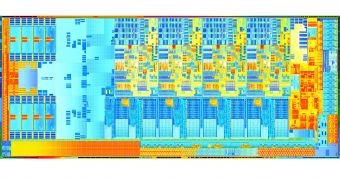
At the moment, Intel is retooling its chip manufacturing process to use larger diameter silicon wafers, for better Ivy Bridge CPU supply. ASML's expertise will help in eliminating potential delays and, eventually, make everything go faster and smoother.
"Productivity improvements driven by enhanced wafer manufacturing technologies, especially larger silicon wafers and enhanced lithography technologies with EUV are direct enablers of Moore's Law, which delivers significant economic benefits to consumers," said Brian Krzanich, Intel senior vice president and chief operating officer.
"The transition from one wafer size to the next has historically delivered a 30 to 40 percent reduction in die cost and we expect the shift from today's standard 300-mm wafers to larger 450-mm wafers to offer similar benefits. The faster we do this, the sooner we can gain the benefit of productivity improvements, which creates tremendous value for customers and shareholders."

 14 DAY TRIAL //