Investigators with the National University of Singapore (NUS) announce the development of a new manufacturing technique for graphene, which is able to produce the 2D carbon-based material at unprecedented rates. This improvement may finally allow the wide-scale use of graphene in electronics.
Graphene was first discovered at the University of Manchester, in the UK, back in 2004, by researchers Andre Geim and Kostya Novoselov, who received the 2010 Nobel Prize in Physics for their work.
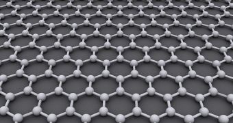
This material is basically an atomic-scale honeycomb lattice made of carbon atoms, which is only one atom thick. Graphene has tremendously exciting physical and chemical properties, so the first decade since its discovery was dedicated to assessing its potential. Nearly 4,000 scientific papers have been written on the material to date.
But now, the focus of studies is slowly shifting from characterization to improving manufacturing. The material was first synthesized from graphite, the carbon compound found in pencil lead. However, for large-scale application, obtaining graphene by peeling single layers of graphite is impractical.
In their approach, NUS investigators sought to mimic the mechanisms employed by beetles and tree frogs, where the creatures can remain attached to leaves even if the latter are submerged. The team was able to both grow and transfer graphene onto silicon, marking the first time this capability is achieved.
Details of the work appear in a paper entitled Face-to-face transfer of wafer-scale graphene film, which is published in a recent issue of the top scientific journal Nature. The main benefit this technique brings is moving away from the former standard approach for growing large graphene films, called chemical vapor deposition (CVD).
CVD uses copper as a substrate for using graphene. This implies a lot of problems, including a low production efficiency – less than that achieved through peeling single layers of graphite – and the fact that the graphene cannot be easily separated from the substrate. Copper also has a tendency to leave impurities in the carbon lattice.
In the NUS face-to-face approach, the copper layer on which graphene grows sits on a silicon substrate. When the hexagonal lattice develops, the copper layer is etched away, and the graphene adheres to silicon via small-scale structures called capillary bridges (the same method used by beetles to adhere to wet surfaces).
“The direct growth of graphene film on silicon wafer is useful for enabling multiple optoelectronic applications, but current research efforts remain grounded at the proof-of-concept stage,” explains Loh Kian Ping, a professor with the NUS Department of Chemistry, quoted by IEEE Spectrum.
“A transfer method serving this market segment is definitely needed, and has been neglected in the hype for flexible devices,” adds the expert, who is also the head of the Department of Chemistry at the university.

 14 DAY TRIAL //