Scientists have finally developed a method that allows them to integrate graphene-based transistors into existing electronic devices, such as cell phones, radios, computers, and laptops.
Adding the innovative, one-atom-thick carbon compound holds great promise for the industry, which may develop considerably as a result. Resulting electronics would be smaller and faster than ever.
But thus far, the unique properties that made graphene such an exquisite choice were also the main obstacles that prevented it from being used in the industry. This is what you would call a paradox.
Now, experts at the University of California in Los Angeles (UCLA) manage to demonstrate a method of allowing such integration, which could ensure that we finally see graphene used in electronics.
Details of the method appear in the September 1 issue of the esteemed scientific journal Nature.
Eliminating these difficulties allowed the UCLA team to fabricate the fastest graphene transistors to date. They could be used to enable high-speed radio-frequency electronics, the team says.
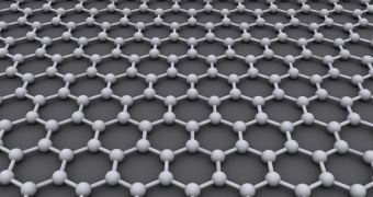
This is because the material, which boasts a honeycomb-like, hexagonal structure, has the highest known carrier mobility level – this is basically the speed at which electronic information is transmitted through it.
Applying existing construction methods to producing graphene always resulted in certain errors making their way into the final product.
The new “strategy overcomes two limitations previously encountered in graphene transistors,” explains Xiangfeng Duan, the UCLA professor of chemistry and biochemistry that led the research effort.
“First, it doesn't produce any appreciable defects in the graphene during fabrication, so the high carrier mobility is retained,” he says.
“Second, by using a self-aligned approach with a nanowire as the gate, the group was able to overcome alignment difficulties previously encountered and fabricate very short-channel devices with unprecedented performance,” he adds.
The expert is based at the UCLA California NanoSystems Institute, where the other two team members, Yu Huang and Kang Wang, also have appointments.
“We are very excited about our approach and the results, and we are currently taking additional efforts to scale up the approach and further boost the speed.” explains UCLA postdoctoral fellow Lei Liao.
Funding for the research came from the US National Science Foundation (NSF) and the National Institutes of Health (NIH).

 14 DAY TRIAL //