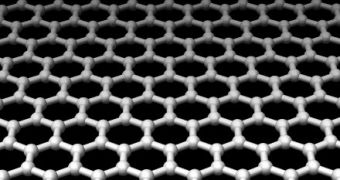
While silicon is the main material used today in computing, because of its high carrier mobility, IBM has been working on an alternative known as graphene. IBM recently announced a breakthrough in the development of graphene field-effect transistors (FETs) and has, even more recently, demonstrated a radio-frequency graphene transistor with a cut-off frequency of 100 billion cycles per second, or 100 GHz.
Graphene is a single layer of carbon atoms, bonded in a hexagonal arrangement similar to a honeycomb. This two-dimensional form of carbon possesses unique optical, mechanical, electrical and thermal properties, which have prompted researchers to intensely explore its technological applications. The 100 GHz frequency record was enabled thanks to wafer-scale, exaspatially grown graphene using a processing technology that is compatible with the one employed in fabricating advanced silicon devices. The 100 GHz frequency is already significantly superior to the one of state-of-the-art silicon transistors, which revolves around 40 GHz.
"A key advantage of graphene lies in the very high speeds in which electrons propagate, which is essential for achieving high-speed, high-performance next generation transistors," Dr. T.C. Chen, vice president, Science and Technology, IBM Research, said. "The breakthrough we are announcing demonstrates clearly that graphene can be utilized to produce high performance devices and integrated circuits."
The high-quality, uniform graphene wafers were synthesized by a thermal decomposition of an SiC (silicon carbide substrate). The graphene transistor was built with a novel gate insulator stack involving a polymer and a high dielectric constant oxide, as well as a metal top-gate architecture. Still, the gate was modest in length, of only 240 nm, but this only means that there is plenty of space for further optimization.
The development of such a transistor is really a key advancement, a milestone, for the DARPA-funded CERA (Carbon Electronics for RF Applications). With this, the goal of creating next-generation communication devices based on graphene is now closer. IBM aims to see graphene transistors even replacing silicon-based ones sometime in the future.

 14 DAY TRIAL //