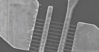
Future generations of integrated circuit interconnects may no longer be made out of copper, if a new technology devised at the Georgia Institute of Technology catches on. Experts have designed a new way of binding the elements inside these circuits, using graphene, thin layers of graphite, only one atom thick. The material can be made at any thickness, with one or multiple layers of atoms overlapping, but has unique and remarkable chemical and physical properties, which make it qualified to go into the next generation of electronic devices. Physicists are convinced that the material is the key to the chips and boards of tomorrow.
The GIT team developed graphene nanoribbon interconnects smaller than 18 nanometers in size, they report in the June issue of the IEEE journal Electron Device Letters. They add that the new material is able to out-perform copper at what it does best, and namely connect transistors and other electrical devices in integrated circuits. Also, the new technology may have the potential to boost the overall processing power of such devices, which apparently has started to reach its peak in silicon-based electronics.
“As you make copper interconnects narrower and narrower, the resistivity increases as the true nanoscale properties of the material become apparent. Our experimental demonstration of graphene nanowire interconnects on the scale of 20 nanometers shows that their performance is comparable to even the most optimistic projections for copper interconnects at that scale. Under real-world conditions, our graphene interconnects probably already out-perform copper at this size scale,” explains GIT Microelectronics Research Center research engineer Raghunath Murali.
He goes on to say that “Resistivity is normally independent of the dimension – a property inherent to the material. But as you get into the nanometer-scale domain, the grain sizes of the copper become important and conductance is affected by scattering at the grain boundaries and at the side walls. These add up to increased resistivity, which nearly doubles as the interconnect sizes shrink to 30 nanometers."
“Even graphene samples of moderate quality show excellent properties. We are not using very high levels of optimization or especially clean processes. With our straightforward processing, we are getting graphene interconnects that are essentially comparable to copper. If we do this more optimally, the performance should surpass copper,” he concludes.

 14 DAY TRIAL //