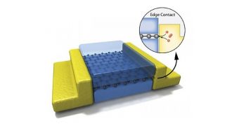
A study published in today's issue of the top journal Science demonstrates an extremely complex method of electrically contacting a bi-dimensional material with a 3D one.
In addition to resulting in the purest graphene ever made, the work also established a new assembly technique for materials constructed from multiple layers, an advancement that will revolutionize materials science for years to come.
The research was conducted by experts at the Columbia University School of Engineering. The team was able to electrically connect graphene, a 2D material, along its uni-dimensional (1D) edge. Previously, such contacts were only possible from the top or bottom of the thin material, not the sides.
In other studies, scientists have attempted to improve the top contact between graphene and other materials by adding dopants, which are chemicals that improve a material's innate electrical characteristics. For example, silicon is doped before it can be used in electronic devices.
The research group made another interesting finding during the study: the issues of graphene contamination and electrical contact are linked. Until now, graphene – a pure 2D matrix of carbon atoms in a hexagonal matrix – always had its properties contaminated by exposure to other chemicals.
In order to maintain these properties, graphene needs to be protected with a 2D insulator. However, since there was no way to link to its edges, the top or bottom of the sheet always had to remain exposed, rendering the insulator moot. With the new advancements, the graphene sheet can be protected thoroughly, leaving only a thin line of single atoms exposed, like in a sandwich.
“This is an exciting new paradigm in materials engineering where instead of the conventional approach of layer by layer growth, hybrid materials can now be fabricated by mechanical assembly of constituent 2D crystals,” says CU Electrical Engineering Professor Ken Shepard.
“No other group has been able to successfully achieve a pure edge-contact geometry to 2D materials such as graphene,” adds the expert, who is a co-author of the paper.
“Our novel edge-contact geometry provides more efficient contact than the conventional geometry without the need for further complex processing. There are now many more possibilities in the pursuit of both device applications and fundamental physics explorations,” Shepard concludes.

 14 DAY TRIAL //