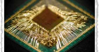
Globalfoundries has just announced that it began installation of special production tools to create 3D-based TSV devices processed on its 20nm technology platform, at its new Fab 8 campus in Saratoga County, N.Y.
We’ve already reported that ATIC, the owner of GlobalFoundries, is heavily investing in 3D chip stacking and TSV technology research.
TSV comes from the electronic engineering concept of “through-silicon via” and is practically a vertical electrical connection (via) (Vertical Interconnect Access) passing completely through a silicon wafer or die.
Fab 8 is currently the most advanced and the largest leading-edge semiconductor foundry in the United States, and they’ve promised they’ll be manufacturing the first full-flow silicon with 3D TVS in Q3 2012.
Of course, these will be sample parts using the company’s advanced 28 nm process, but they might be the first 28 nm TSV chips in the world.
There are many fabless IC designers out there such as Nvidia or Qualcomm that will likely be very interested in the TSV chips GlobalFoundries will be able to offer next year.
The company is installing special production tools to create 3D-based TSV devices in Fab 8, which is their newest 300mm fab in Malta, N.Y. These tools will enable 3D designs at the 20nm node, with vias having a 6nm diameter and 40-to-50u pitches.
As we’ve already said, the first 3D stacked chips won’t be manufactured in the 20 nm process. The initial products, including chipsets and GPUs, may start production in 2013.
They’ll likely be made in 28 nm, while the 20 nm 3D chips will come in full production in 2014.
The semiconductor company is pursuing both the 2.5D and 3D TSV foundry markets.
GlobalFoundries is already implementing simple stacking configuration that's often called 2.5D at their Singapore FAB. This method takes advantage of TSVs by running them through an intermediate layer of silicon called an interposer.
Xilinix is one of the pioneers of the interposer concept and they’ve already managed to get a four level FPGA containing 7 billion transistors.
Depending on how hot the chips get, designs with multiple stacked dies will revolutionize the chip design world.
Low power chips are much easier to stack, as they dissipate a smaller amount of heat. Having high heat dissipation is not compatible with the chip stacking concept as the TSV method dramatically increases chip complexity and makes reliable cooling almost impossible.

 14 DAY TRIAL //