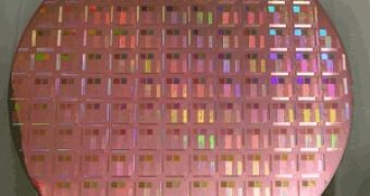
One of the biggest, if not the biggest semiconductor manufacturing facility in Taiwan is the TSMC- they are the suppliers for an entire industry and, basically, millions of people use products that they made, and probably don't even realize it. As one of their main concerns is to keep up with the industry's demands, and sometimes even to be a step ahead of where everybody asks them to be, just to maintain the superiority on the market they have struggled for so long to achieve.
Part of this constant need of improvement has to do with the manufacturing process they use to make different products and the clients knocking on their door. One of their big customers is Intel; they have planned the next generation of Core processors, codenamed Penryn, to hit the market somewhere in the third quarter of this year, with full scale production being expected for the beginning of 2008.
TSMC also hopes of rising to the challenge by entering the 45nm process node in September, with estimations already made in production scaling; they planned on having twice the density of 65nm with lower power and manufacturing cost per die. The 45nm process node combines the 193nm immersion photolitography, performance-enhancing silicon strains and extreme low-k (ELK) inter-metal dielectric material.
Dr. Rick Tsai, president and CEO of TSMC said: "Customers expect both performance and reliability from TSMC, a fact that has guided the development of our 45nm process every step of the way. With 45nm solution ready and production to be started in September, TSMC provides next-generation technology at the earliest possible time."
The manufacturing process is able to stuff together more than 500 million transistors onto a 70mm2 die area. There are three processes that are being planned by TSMC, the first will be the Low Power (LP) 45nm process, followed by the General Purpose and High Performance (GS) process and the Low-Power triple Gate oxide (LPG).

 14 DAY TRIAL //