Discovering all there is to know about graphene is one of the most important goal in physics and chemistry today. The amazing properties this material has make it a suitable choice for replacing silicon in electronic devices, but experts are not yet familiar with all of its properties. One of the challenges in the field was developing a good graphene noise model, which would allow experts to create materials with strong signals and weak background noises. This has recently been accomplished by a research team featuring experts from multiple research institutes and organizations.
Graphene has a single-atom-thick crystalline structure, which sees carbon atoms being arranged in a honeycomb-like, hexagonal pattern. This allows electrons to flow through the material at nearly the speed of light, which is about 100 times faster than the speed electrons can take inside silicon. In addition, the carbon compound is also very resistant to mechanical stress, and highly flexible too. This means that it could be used for both “common” and flexible, bendable and stretchable electronics as well. This prospect makes the material extremely interesting to the scientific community.
“In this work, we present the four-probe low frequency noise characteristics in single- and bi-layer graphene samples, using a back-gated device structure that helps simplify the physics in understanding the interactions between the graphene and the silica substrate,” says Yuegang Zhang, a materials scientist at the US Department of Energy's (DOE) Lawrence Berkeley National Laboratory (Berkeley Lab). The team based its researches at the facility's Molecular Foundry division.
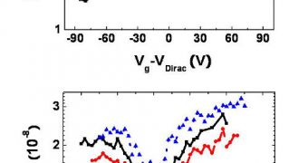
“For single-layer graphene we found that the noise was reduced either close to or far away from the lowest electron density of states, sometimes referred to as the Dirac point for graphene, forming an M-shaped pattern. For the bi-layer graphene, we found a similar noise reduction near the Dirac point but an increase away from that point, forming a V-shaped pattern. The noise data near the Dirac point correlated to spatial-charge inhomogeneity,” Zhang adds.
The Foundry had the necessary equipment to allow the group to conduct its study. It was discovered that the signal noise level in graphene is lowest near the region featuring the least electron density of states. This is the area where the number of energy states available to each electron is the lowers possible. The team published its findings in a paper entitled “Effect of Spatial Charge Inhomogeneity on 1/f Noise Behavior in Graphene,” which appears in the latest issue of the esteemed scientific journal Nano Letters. Funding for the work came partially from the DOE Office of Science.

 14 DAY TRIAL //