Physicists and materials scientist around the world are currently working on developing methods of including graphene inside next-generation electronics without causing the material to lose its trademark physical and chemical properties. The effort is bound to be very challenging, experts say.
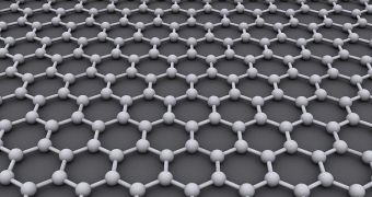
The reasons why so many electronics experts look up at graphene is its way of handling the flow of electrons making up electricity. The material features a straight, flat, 2D structure, that allows electrons to move through it at speeds up to 100 times higher than those achievable in silicon.
As such, engineers say that graphene is the next best thing for electronics. But actually using the carbon compound in such applications is not as easy as it would first appear. Graphene is apparently not really a team player.
Scientists at the US National Institute of Standards and Technology (NIST) say that the material starts experiencing a reduction in the amount of electrons it can carry as soon as it is placed in devices, and sandwiched between layers of other materials.
The reasons why that happens is because imperfections in the way the materials are put together are causing massive valleys and steep hills to develop on the graphene surface. This in turn prevents the smooth flow of electrons from one end of the graphene area to the other.
But its precisely this obstacle that could make the new material an ideal candidate for probing interactions between electric conductors and insulators, the NIST experts write in the latest issue of the esteemed scientific journal Nature Materials.
These studies could be conducted using an observations technique called scanning tunneling microscopy (STM), says NIST Fellow Joseph Stroscio. He adds that researchers need to isolate the material from its environment, if they want to use it fully.
“To get the most benefit from graphene, we have to understand fully how graphene's properties change when put in real-world conditions, such as part of a device where it is in contact with other kinds of materials,” Stroscio explains.
“What we found [in STM studies] is that variations in the electrical potential of the insulating substrate are interrupting the orbits of the electrons in the graphene, creating wells where the electrons pool and reducing their mobility,” says Nikolai Zhitenev, also a NIST scientist.
Studies will undoubtedly discover a way of smoothing graphene inside future electronic devices, as science simply cannot afford not to use this material. Graphene was discovered in 2005 by experts at the University of Manchester, in the UK, EurekAlert reports.

 14 DAY TRIAL //