14 DAY TRIAL //
 EVGA has released recently the first pictures of the company's upcoming GeForce GTX 580 Classified graphics card that it will be based on a heavily customized in-house design meant to cater to the needs of extreme overclockers and enthusiasts.
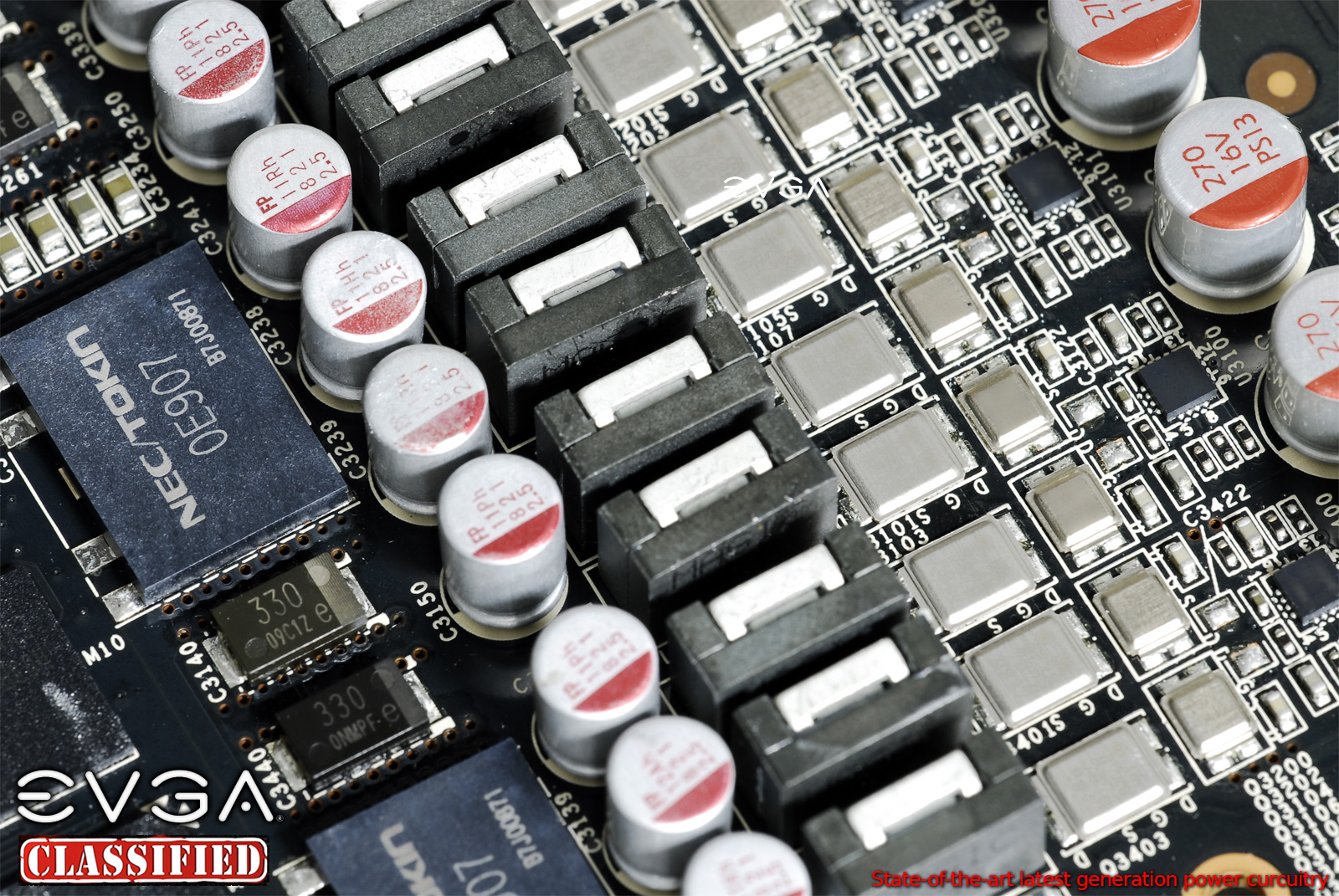
The first thing that one notices when taking a look at EVGA's upcoming creation is that the card uses a higher than average PCB as well as a blower type cooling system.
The tall printed circuit board was required for installing the beefed-up power delivery circuit used for the GeForce GTX 580 Classified, which uses high-quality components and a couple of Nec/Tokkin proadlizer film capacitors for added voltage stability.
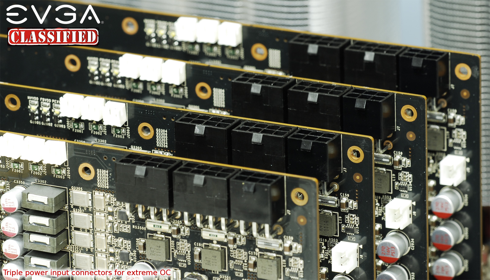
Power is drawn from the PSU via two 8-pin and one 6-pin PCI Express connectors. EVGA has used a similar configuration for the GTX 285 Classified, where the 6-pin plug was dedicated to the memory.
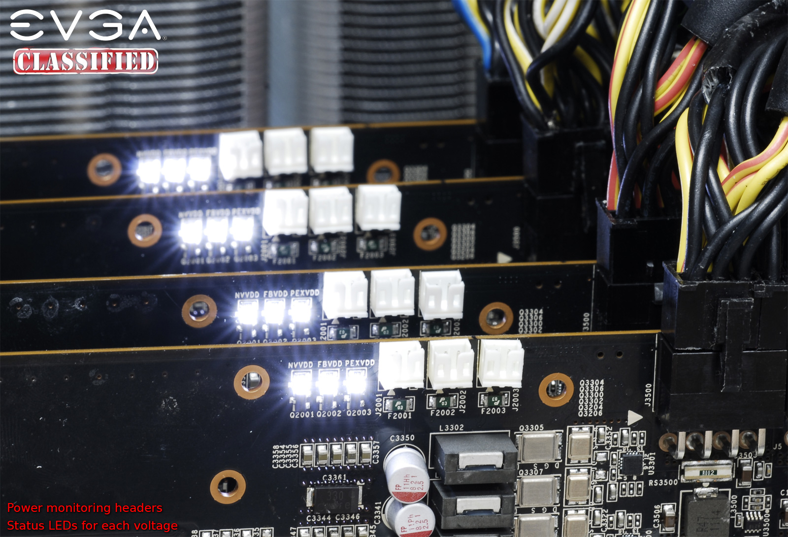
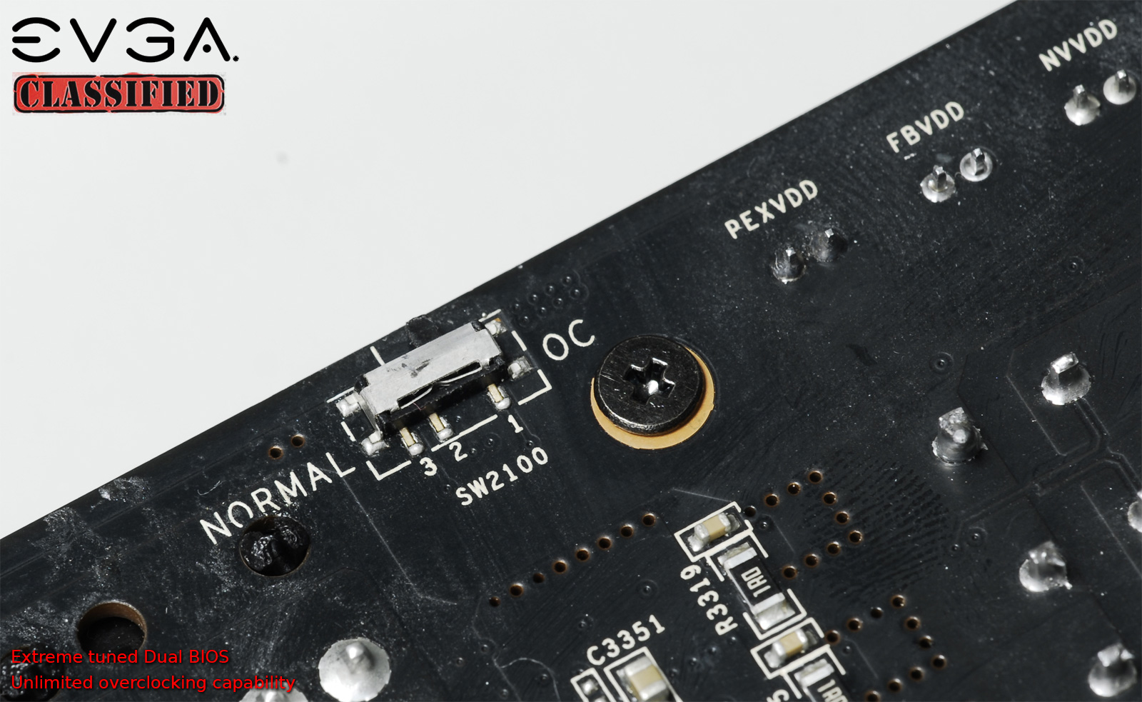
Just as is the case with most other overclocking-oriented graphics cards, the EVGA GTX 580 Classified includes a series of on-board voltage read points as well as dual BIOS chips.
Users can change between the various settings saved in the BIOS files via a switch that is placed on the back of the PCB.
Other overclocking friendly features include three power monitoring pin headers and a series of status LEDs for the card's main voltages.
The GTX 580 is based on Nvidia's GF110 GPU that packs 512 stream processors, 64 texture units, 48 ROP units, and a 384-bit memory interface that is linked to a 1.5GB GDDR5 frame buffer. Its default clock speeds are set at 772MHz for the GPU and 1002MHz (4008MHz data rate) for the memory.