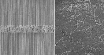
Producing carbon nanotubes is easy - scientists cracked that secret more than a decade ago, albeit making them grow in an orderly fashion is somewhat more complicated. Or at least it was, because two teams of researchers have recently proven new methods through which carbon nanotubes can be sorted and organized so that they can be successfully used to create new high performance electronic devices.
The two main disadvantages with current electronics is that they are built mostly using two types of materials, conductors and semiconductors, and that the physical limit to chip minimization is already drawing nearer. Semiconductors have given us all there was to give but now it's time for a change. Not only that carbon nanotubes provide the solution to the problems regarding minimization, but they can also be used to create both conductor and semiconductor materials.
The current technology used to develop carbon nanotubes however, is mostly flawed by the fact that it relies largely on luck. The nanotubes will grow eventually, but there is no way to control the processes that can make a carbon nanotube exclusively conductor or semiconductor, nor can their shape be influenced.
"An ant is incredibly strong for its size. But nobody uses ants to do useful work, because they all run around in different directions," says Mike Mayberry, the director of component research for Intel.
Thus, ever since they have been discovered, scientists have been struggling with nanotubes of all sizes, shapes and molecular structures. A carbon nanotube is basically a microscopic cylinder with single or multiple walls formed of 'sheets' of interlocked carbon atoms. They can grow as thin as one nanometer in diameter and up to a couple of centimeters long, resulting in structures with a ratio of 30 million to one between length and width.
Because they are basically held together only by atomic bonds, carbon nanotubes are extremely strong and have exceptional electrical properties at the same time; in the end, whether a carbon nanotube becomes a good conductor or a semiconductor depends only on the way the carbon sheet is rolled up.
Carbon nanotubes can become useful to the semiconductor industry only if they can be integrated on silicon chips. Growing them directly on the silicon wafer ultimately results in disordered patterns, although researchers from Stanford's electrical engineering department have revealed in a paper last month that this problem can be easily solved if the tubes are grown on crystalline quartz. This creates orderly rows of carbon nanotubes which can then be transferred onto silicon chips, to create a working electronic device.

 14 DAY TRIAL //