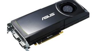
While there are already quite a number of GeForce GTX 580 cards out in the open, now that NVIDIA's various partners let their inventions loose, none of them can truly claim to be capable of what ASUS seems to have pulled off.
For those interested in a reminder, the GeForce GTX 580 is NVIDIA's new Fermi board, based on the GF110 40nm graphics processing unit.
Various hardware makers have already contributed with their own stock-clocked or factory overclocked models.
ASUS, however, tried to make the newcomer especially appealing to enthusiasts, particularly those seeking to perform unusual overclocking feats.
Thus it was that the GeForce GTX 580 Voltage Tweak was born, an adapter whose factory overclocking is supplemented by direct control over the GPU frequency.
As end-users may know by now, the new graphics adapter has 512 CUDA cores, 1,536 MB of GDDR5 VRAM and a memory interface of 384 bits.
The GTX 580 Voltage Tweak has frequencies of 782 MHz for the GPU, 1,544 MHz for the shaders and 4,008 MHz for the memory.
Still, by means of the Voltage Tweak feature, users can supposedly push the clock of the GF110 graphics processor all the way up to 1,157 MHz.
Basically, this corresponds to a performance boost of about 50 percent compared to NVIDIA's original creation.
Of course, the rest of the feature set still includes DirectX 11 support, CUDA, PhysX, 3D Vision and SLI (for multi-GPU configurations).
When in SLI, users can even enjoy games and multimedia playback on three screen simultaneously, by virtue of 3D Vision Surround.
As for connectivity, there are two DVI ports present, as well as a mini HDMI 1.4a connector, while power is delivered through an 8-pin and one 6-pin PCI Express power connectors.
Pre-orders should already be possible, though customers will have to part with 469 Euro.

 14 DAY TRIAL //