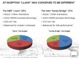
AMD's upcoming Llano architecture will take the company's Fusion concept to a whole new level as the fastest APUs to be released are more GPU than CPU, according to a recent report.
This becomes apparent when taking a look at the die budget of Llano as almost half of the APU's transistors are dedicated to the on-board graphics core, while the remaining die space is split between the x86 cores (including cache) and the northbridge.
Such a large die area needs to be dedicated to the graphics and media engines since the GPU used by Llano is derived from AMD's Radeon HD 6000 series of video cards that sport full DirectX 11 compatibility and other advanced features including the UVD3 media decoder.
In addition, the Radeon HD 6550 GPU that is used for the company's fastest APUs, the A8-3560P and the A8-3550P, packs no less than 400 stream processors, the same number of SPs used in the Radeon HD 5670.
These will be clocked at 594MHz and the HD 6550 also features support for a technology similar to Hybrid CrossFireX that allows for the CPU integrated graphics to be used together with a Turks-based graphics card in order to increase the performance of the system in games and GPGPU applications.
Working in this mode, the two graphics chips should behave similarly to a Radeon HD 5770/6770, which should make such a setup well suited for some 1680x1050 action.
Llano APUs are based on the K10.5+/Husky x86 architecture and outside of the on-die graphics also feature an integrated dual-channel DDR3 memory controller, a PCI Express controller, up to 4MB of cache and select processors pack AMD's Turbo Core 2.0 dynamic acceleration technology.
The initial launch, that is planned to take place later this quarter, will include at least four quad-core and one dual-core desktop chips as well as a series of mobile parts. (via Sweclockers)

 14 DAY TRIAL //
