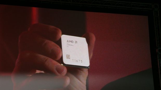
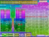
In the first half of this year, AMD is expected to unveil its next-gen APUs based on the Trinity architecture and recently a die shot of such a chip was published on the Web revealing some new details about AMD’s upcoming creation.
On a first look, the die itself looks to be extremely different from that of Llano and one of the most obvious changes is that the chip doesn’t used quad Stars processing cores as its predecessor, but rather two AMD Bulldozer modules packing four Piledriver cores.
These are placed in the left part of the die and above them stand 4MB of L2 cache (2MB for each module) as well as a dual-channel DDR3 memory controller supporting memory speeds up to 2133MHz.
The PCI Express controller is placed at the bottom of the chip and seems to support the same number of PCIe channels as Llano, while between the two Bulldozer modules stands the hardware logic that would have traditionally made out the North Bridge.
Taking a look at the right part of the die, we get to see Trinity’s integrated graphics core.
Although no details are provided, from the look of it the built-in GPU seem to be packing 6 VLIW4 shader clusters for a total of 384 Radeon cores.
While the shader count is smaller than that of Llano (384 vs 400), the VLIW4 architecture used by Trinity is more efficient than the previous VLIW5 design utilized in the Llano Arch.
The clock speeds of the integrated GPUs used for Trinity are also expected to be higher than that of Llano, and AMD estimated that these modifications will make the new chips up to 30% faster when running graphics tasks than their predecessors.
According to SemiAccurate, the whole die area on the Trinity APU will span approximately 240 square mm, which makes it slightly larger than Llano that measures 228 square mm.

 14 DAY TRIAL //

