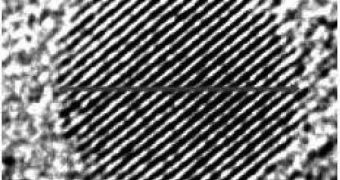
While current microprocessor architectures can provide researchers with vast amounts of computational power, there is no doubt that the future of processing is in 3D architectures. Scientists at the Stanford University have recently developed a new way of making that possible, when they have created a method of stacking and purifying germanium nanocrystal layers. The innovation could contribute significantly to the goal of designing a 3D processor, able to handle much more information than the most advanced, single-layer one, PhysOrg reports.
In the new process, small germanium crystals were arranged as nanowires on a silicon substrate. On top of them, another layer of germanium was set. Then, the entire mix was subjected to heat. This caused the germanium to take on the crystalline shape of the silicon underneath, essentially resulting in a 3D integrated circuit. The new method, which is a lot simpler than other ones, could be the cheap and sustainable answer to the dilemma of how to place germanium on silicon, which physicists are trying to answer.
“We can make very long and very small single crystals and, in principle, place them where they are needed on a surface. We use them as seeds to purify noncrystalline layers on top of the level of silicon and, therefore, control the perfection and orientation of those overlying layers,” the Director of the SU Geballe Laboratory for Advanced Materials, Paul McIntyre, explains. He is also one of the four researchers in the team involved in the new experiments. The expert adds that the main goal of such studies is to develop a method of placing pure nanocrystals in 3D circuits, in a manner that ensures the smoothest electron flow between the layers possible.
“Many scientific groups are trying to find something that will have more computing power, higher speed, lower energy consumption, and could continue to scale down for many years to come,” McIntyre says. For the perfect arrangement, “We have to find some clever way of depositing a layer that isn't a single crystal by purifying it so that it shares the perfect orientation of the silicon substrate,” the expert adds. In his team's approach, the nanocrystals are interconnected with a vast amount of nanowires, which ensures a smooth current flow between circuit layers.
“Producing a potential electrical connection through the nanowire is quite unique. The ability to access each of these devices individually from layer to layer in an easy way is one thing that many people would like to have,” he concludes.

 14 DAY TRIAL //