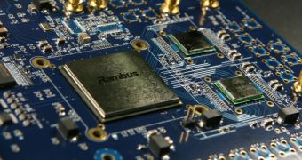
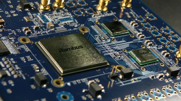
The Terabyte Bandwidth Initiative (TBI) is now official, as Rambus has succeeded in delivering their first functional TBI prototype to feature data rates of 16Gbps at a bandwidth of one terabyte per second (TB/s). Rambus will be the first to implement the technology on the current world's fastest memory, the Rambus 4.8GHz XDR? DRAM, in order to achieve dramatically increased memory data rates.
The TBI prototype is made of three 65nm, chips, a SoC stand-in and two simulated DRAMs. Rambus tried to reproduce all the features of a DRAM module that might exist in the near future (2010-2011). Upon this prototype, Rambus engineers were able to get a potentially usable signal between the SoC and the DRAMs at a 32x data rate. However the signal is somehow altered and would require filtration.
"We will drive memory signaling technology to performance levels that are an order of magnitude greater than what can be achieved today," said Kevin Donnelly, senior vice president of engineering at Rambus Inc.
The Terabyte bandwidth Initiative includes other innovations, such as 32X data rate - 32 data bits per input clock cycle, Fully Differential Memory Architecture (FDMA) - industry's first differential signaling for both data and command/address (C/A) as well as FlexLink? C/A - The industry's first full-speed, point-to-point C/A link.
"Continuing the Rambus tradition of innovation, our engineers and scientists have pioneered new technologies that will enable terabyte per second memory architectures for gaming, computing and consumer electronic systems of the next decade", continued Donnelly.
Rambus has a long, 17-year tradition in challenging memory technologies through technology development programs. Until now, Rambus has developed innovations resulting in over 1000 issued and pending patents worldwide.
The Rambus Terabyte Bandwidth Initiative is expected to be fully ready for large-scale implementation until 2010.

 14 DAY TRIAL //
