14 DAY TRIAL //
 As you probably remember if you read this, yesterday we started to report on what, by now, seems to be an excruciately long disassembly process, meant to reveal the inner-workings of Sony's Google TV enabled NSX-24GT1, the guys from Nikkei Electronics Teardown Squad reaching step two of this process, to find out what makes this Android powered platform tick.
For a quick refresher course in what happened yesterday I suggest you to read our previous report detailing how did the Nikkei Electronics team got where they are today, since now we are going to take a closer look at the TV board that goes inside the NSX-24GT1.
This is just one of the three different boards that are to be found inside Sony's TV and its used for managing the TV functions of the unit.
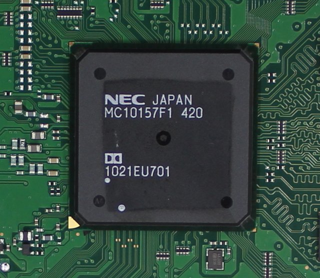
After what can be described as a strange method of removing a heatsink (that actually required adding more solder to the board), the TV board revealed all its secrets, the TV functions being controlled by a Renesas Electronics SoC that carries the part number MC10157F1, the guys over at Nikkei Electronics saying this is actually an EMMA3TL2 image processing SoC, supporting worldwide digital/analog broadcasting formats (ATSC for the US, DVB for Europe and ARIB for Japan).
Furthermore, this chip also supports a wide range of audio formats, virtual surround, MPEG-4 AVC/H.264, VC-1, AVS, DivX-HD video decoding, Full HD deinterlacing, to name just a few of its features.
Unfortunately this is where this episode ends, so we still don't know what is actually hidden behind that hefty heatsink that covers the Android board, although I have a feeling this won't actually take that long to find out since there's hardly anything left to teardown in Sony's NSX-24GT1 TV.
So, keep your fingers crossed and hope the third part, will actually be our last one.