14 DAY TRIAL //
 After a long wait, Intel second generation Core processor family, code named Sandy Bridge, is finally out for us all to witness, so it's time to take a look at these new CPUs and see what all that hype built around them is about.
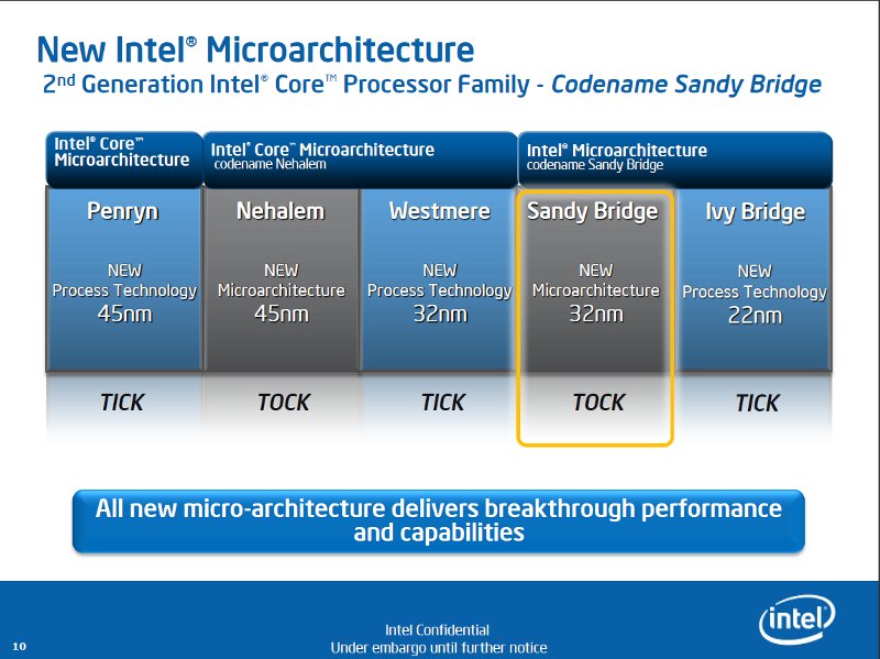
As certainly all of you already know, since 2007, all of Intel's processors are developed on what the company calls a tick-tock product cycle.
What this basically means is that every CPU architecture change (tock) is followed by a die shrunk version of the same core, called a tick.
Every year, there is expected to be one tick or tock.
Since last year during CES 2010, Intel introduced the Westemere processor that was based on the company's 32nm manufacturing process, now it's time for a new architecture to make its introduction to complete the tick-tock cycle.
This new processors microarchitecture is called Sandy Bridge, or the second generation Core processor family as Intel likes to refer to it, and could actually be considered an improved Westmere, since it takes some of the features introduced by Intel back in January 2010 and takes them one step further.
This means that we now get better CPU integrated graphics, improved clock speeds as well as the second generation Turbo Boost technology, to name just a few of the changes introduced by Sandy Bridge.
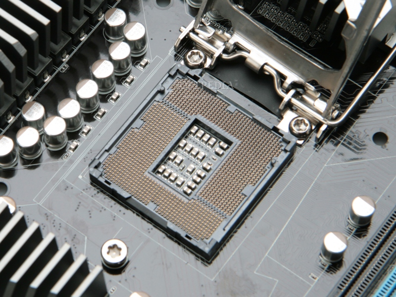
Together with all of these, we also get a new socket, called LGA 1155, so Sandy Bridge CPUs won't be a drop-in Westmere update, but will require a whole new motherboard.
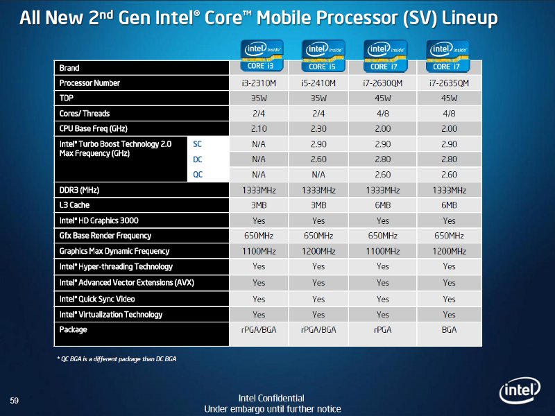
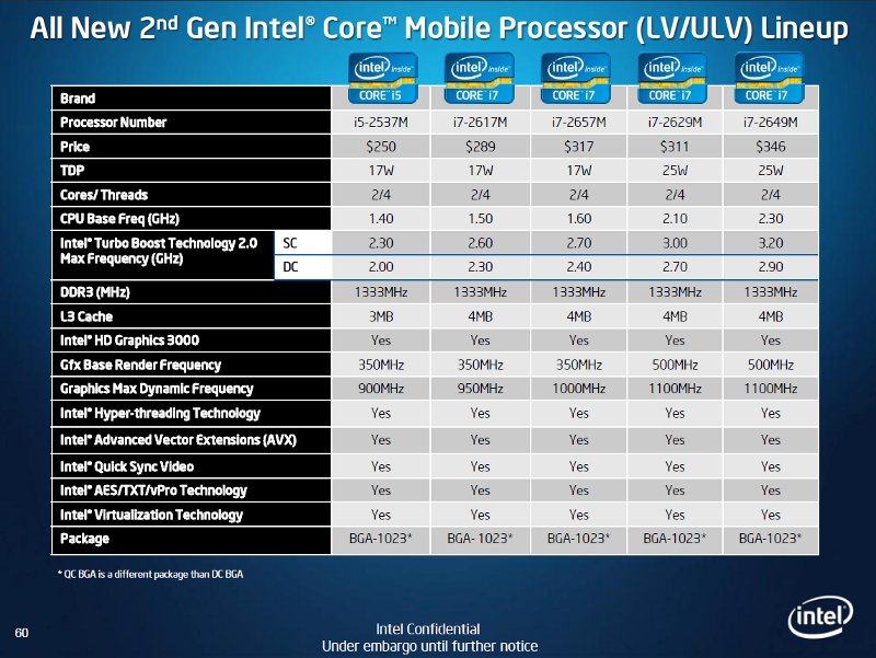
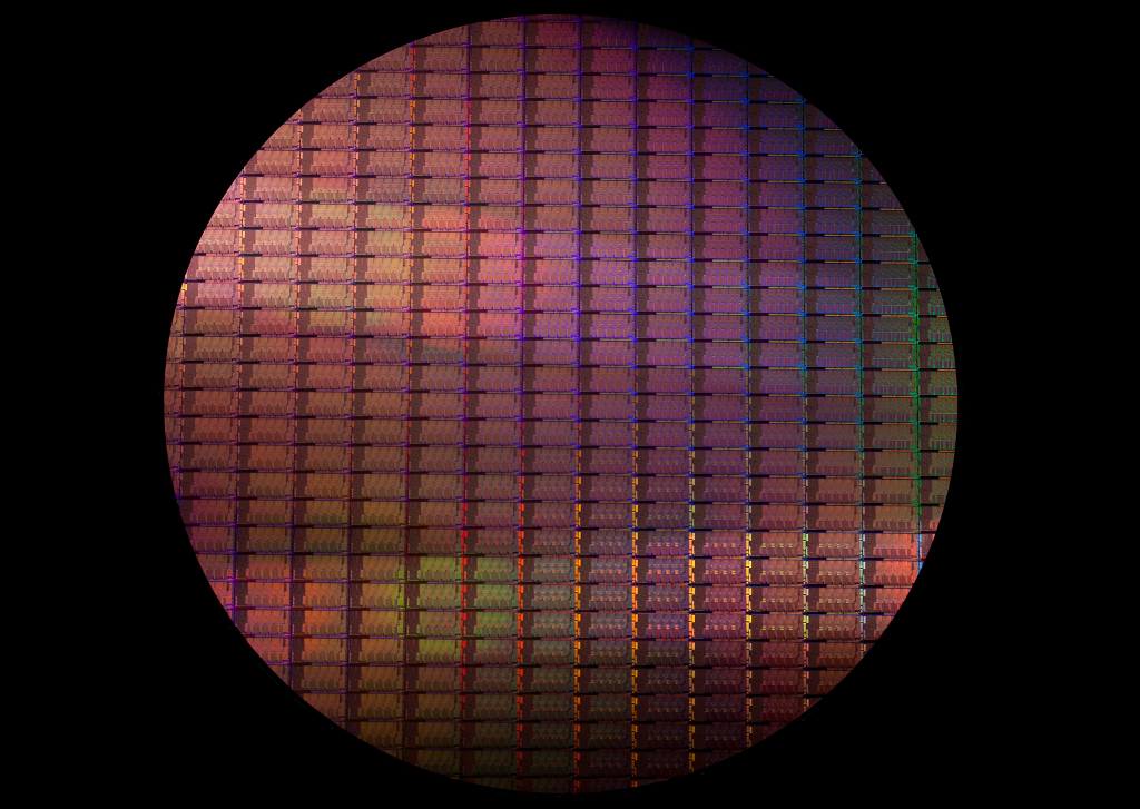
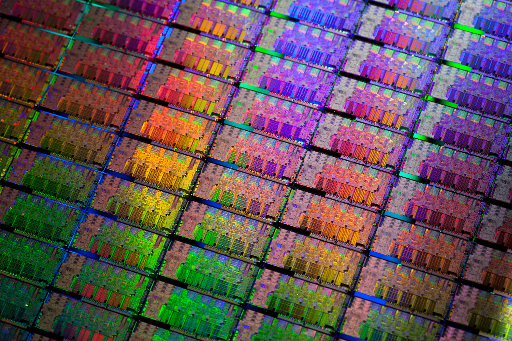
Although the Sandy Bridge architecture is new, Intel is launching today no less than 29 new processors, most of these being especially designed for notebooks.
Ranging from dual-core to quad-core models, the mobile Sandy Bridge part list is split into two different branches, Intel releasing regular voltage CPUs as well as low-voltage and ultra low-voltage models.
The complete list with the laptop parts available today is included bellow, the regular voltage mobile processors featuring 35W, 45W and 55W TDPs, while the LV and ULV SKUs are rated at a much lower 17W or 25W power draw.
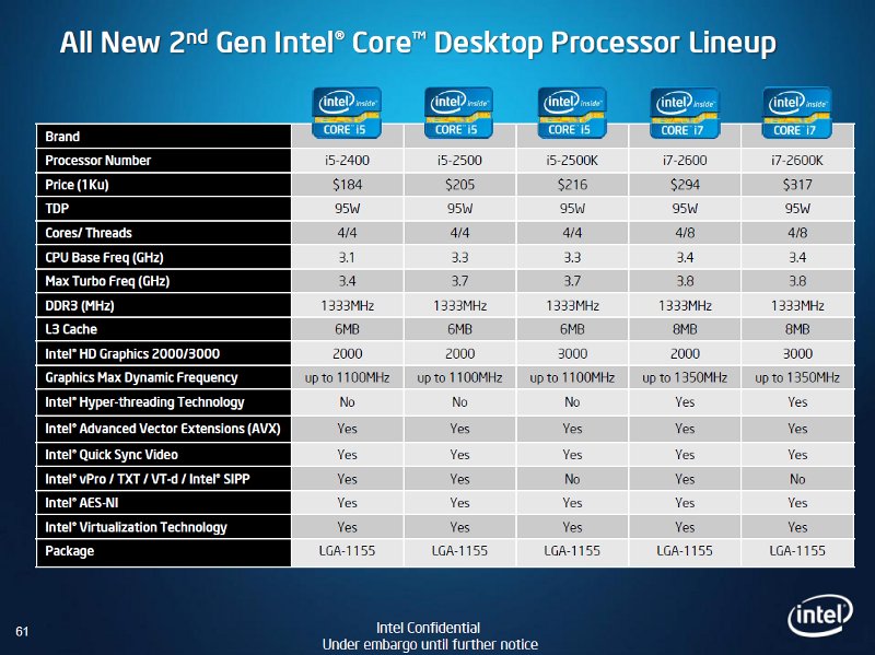
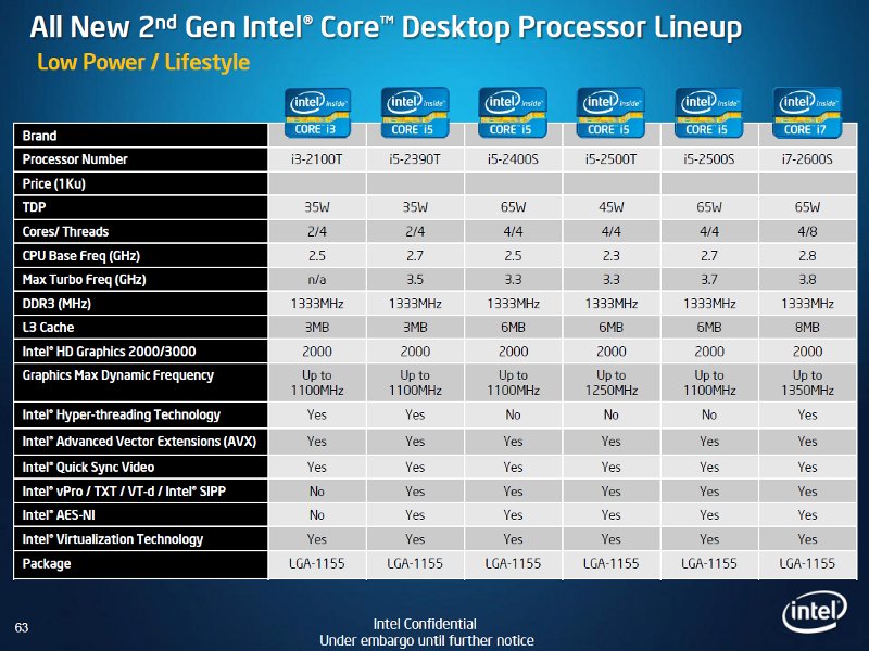
Moving to the desktop sector, these too are split in two sections, Intel developing a so-called “Low power/lifestyle” CPU category that is destined to make its way into All-in-One PCs and other such computers.
Compared to the regular desktop CPU lineup, these have lower operating frequencies and a lower power draw.
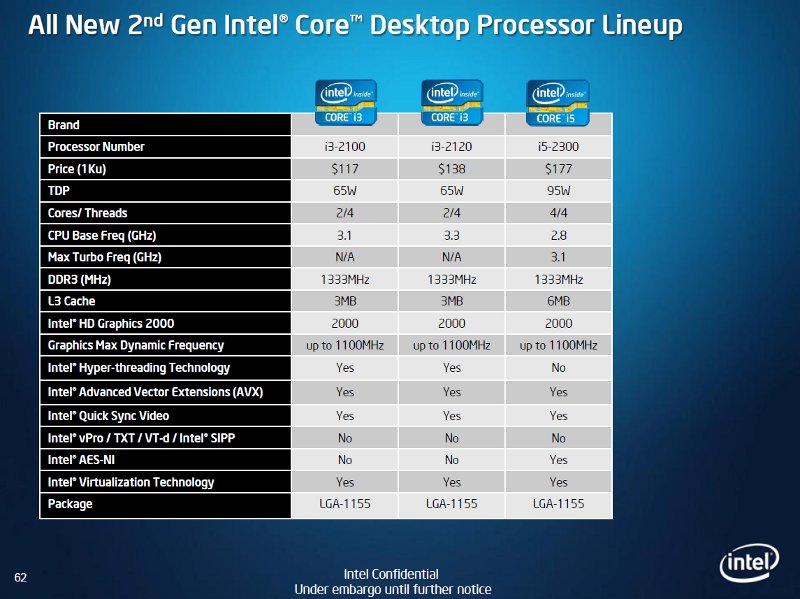
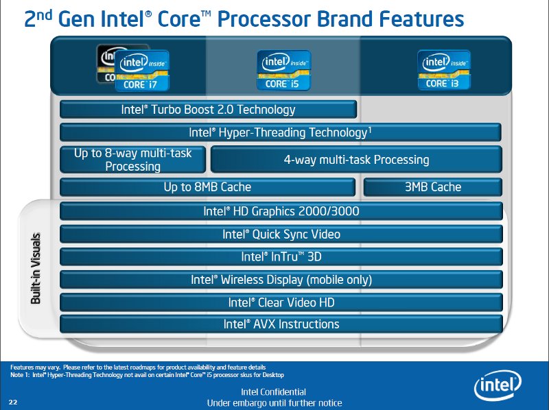
The rest of the desktop lineup is made out of another eight processors, two Core i3, four Core i5 and two Core i7 models.
Going from top to bottom, the Core i7 2600 and 2600K feature quad operating cores, have an 95W TDP, 8MB of Level 3 cache memory and support Intel's Hyper-Threading and Turbo Boost technologies.
The Core i5 models drop Hyper-threading support, so they can “only” execute four threads at a time, but still carry Turbo Boost.
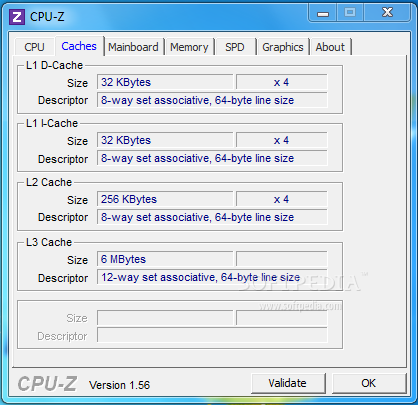
The TDP has remained unchanged, being estimated at 95W, but the cache memory was reduced to 6MB.
Finally, we get to the two Core i3 models that feature a dual-core design and drop Turbo Boost and AES-NI encryption.
The L3 cache is cut in half compared to the Core i5, but Hyper-Threading is enabled so the OS sees these as quad-core processors.
Reducing the number of cores also means that both Core i3 CPUs have a lower TDP, this being estimated at 65W.
You can take a look for yourself at the desktop Sandy Bridge processor lineup just below.
Since a new platform is required for Sandy Bridge, together with all these new CPUs, Intel is also introducing ten new motherboard chipsets, five for desktop and five for mobile computers.
Besides the already popular P67 and H67 chips, desktop users can also choose from Q65, Q67 and B65 based motherboards, while laptop manufacturers will have the option of using the QS67, QM67, HM67, HM65 and UM67 chipsets.
Sandy Bridge architecture
As stated earlier, Sandy Bridge is a new architecture for Intel, so quite a few things are different compared to the previous Westmere chips, although they are both based on the same Nehalem design that was launched more than two years ago.
Since all these details were released by Intel during the company's Fall IDF, the information was already out in the open and analyzed in detail by various websites.
But this won't stop me from presenting you the most important changes that have occurred since the Westmere core.
I'll start things off with the Sandy Bridge front end, where all the instructions are handled by the processor.
The fist change operated by Intel to this part of the chip was to add a so-called “L0 instruction cache” to the decode path that caches instructions as they are decoded and features an 80% hit rate for most applications.
This means that every time the chip receives an instruction it will first check to see if this is found inside this micro-op cache, effectively cutting down power consumption and increasing performance if the instruction is found.
Furthermore, together with this micro-op cache, Intel also introduced a redesigned branch prediction unit that can hit twice as many targets and features a much more effective storage for its history.
All these changes have lead to more accurate predictions while maintaining about the same die footprint as its predecessor.
Moving on, another significant change that Intel introduced in Sandy Bridge is a physical register file, thus reducing the Out-of-Order (OoO) processing hardware required as the chip has only pointers to move along with the instructions processed (effectively cutting down on the die size necessary for OoO execution hardware).
As Intel points it out, this was the key for enabling Advanced Vector Extensions (AVX) in Sandy Bridge.
Suitable for floating point-intensive calculations in multimedia, scientific and financial applications, AVX instructions provide increased parallelism and throughput in floating point SIMB calculations.
In Sandy Bridge, AVX instructions support 256-bit operands and effectively double the chips peak floating point performance.
In order to keep up with this increased bandwidth, Intel has enhanced the design of its load/store units, the two ports having a symmetric design as each of these can act as a load or store address.
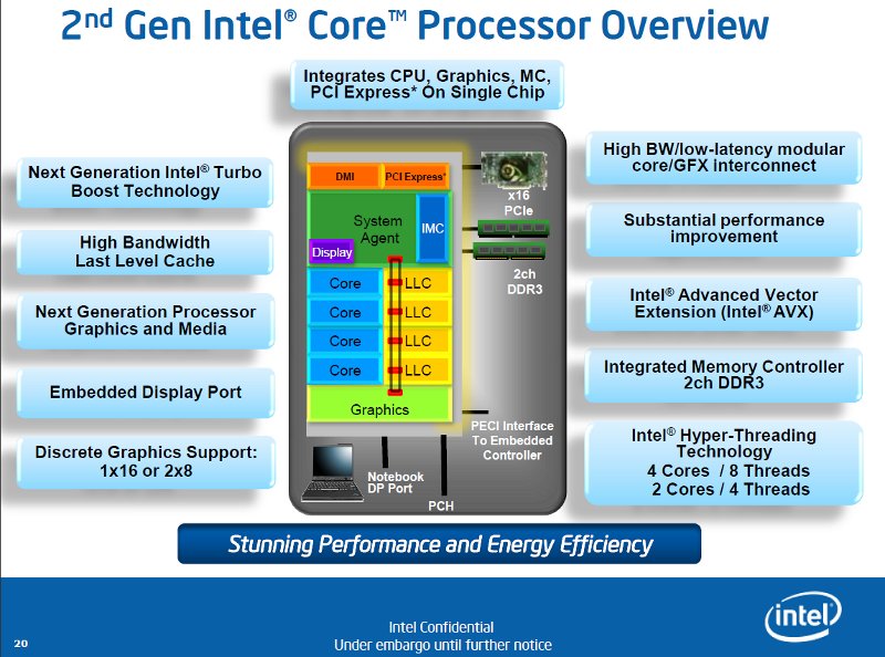
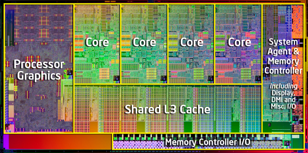
Another major design change that Intel introduced together with the Sandy Bridge is the introduction of a ring bus that connects the Level 3 cache together with all the processors cores as well as with the integrated graphics and with the so-called System Agent (ex Un-core).
This approach simplifies CPU design as it eliminates the need for adding another 2000 wires to Sandy Bridge in order to connect the L3 cache with the integrated GPU.
Furthermore, cache latency has been reduced and the speed increased as the L3 cache is now clocked at the same speed as that of the rest of the CPU.
Divided into slices, as each core gets its own L3 cache memory, every cache segment has a full cache pipeline.
Speaking of the System Agent, this gets 16 PCIe 2.0 lanes that can be split into two x8 connections and features a redesigned DDR3 memory controller, its clock speed being lower than that of the processor.
But the most interesting part about the Sandy Bridge architecture is the new integrated graphics unit that delivers an important IPC (instructions per clock) increase.
Unlike Westmere, the GPU is built on the same die as the CPU and gets access to the processor's L3 cache.
However, it gets its own power and clock plane as well as a Graphics Turbo mode.
The shader hardware is composed of a mix of shaders, cores and execution units that make up an EU.
Sandy Bridge processors can come with either 6 or 12 such EUs (this being the difference between the Intel HD 2000 and HD 3000 graphics units), all mobile models getting 12 EUs, while desktop processors can get 6 or 12, depending on the model.
Together with the new integrated graphics, Sandy Bridge also received a media engine that is now capable of hardware accelerated video encoding.
Called the Intel QuickSync technology, this new part of the chip is able to transcode a wide array of video files and supports resolutions as high as 1080p.
Another significant change was made to the Turbo Boost technology that has reached version 2.0 and is capable of shortly exceeding the TDP of the chip, enabling it to achieve even faster clock rates.
In its previous iteration, Turbo Boost presumed that once it increases the clock speed of a core, this will immediately reach its maximum TDP.
However, this is rarely the case in practice as it usually takes some time for the CPU to dissipate that much heat, so this new technology monitors the heat output of the chip and allows it to operate over its TDP for short amounts of time, usually a few seconds.
In addition, GPU and CPU Turbo modes are interconnected, so the processor can increase the CPU clock speed and decrease the GPU frequency when a processor intensive task is run and vice versa.
All these improvements should allow Sandy Bridge to perform a lot better than Westmere and Lynnfield, but there is one area where Intel decided to be a lot more conservative.
I am talking, of course, about overclocking support since, as everybody knows by now, Intel has locked the BLCK frequency of its Sandy Bridge processors, allowing only for multiplier overclocking in some of its processors.
I say some since only the K series CPUs come with a fully unlocked multiplier, the rest of the CPUs featuring a multi limit while others get a fully lock multiplier, overclocking being effectively impossible on these latter chips.
Hardware Specifications and Testing Methodology
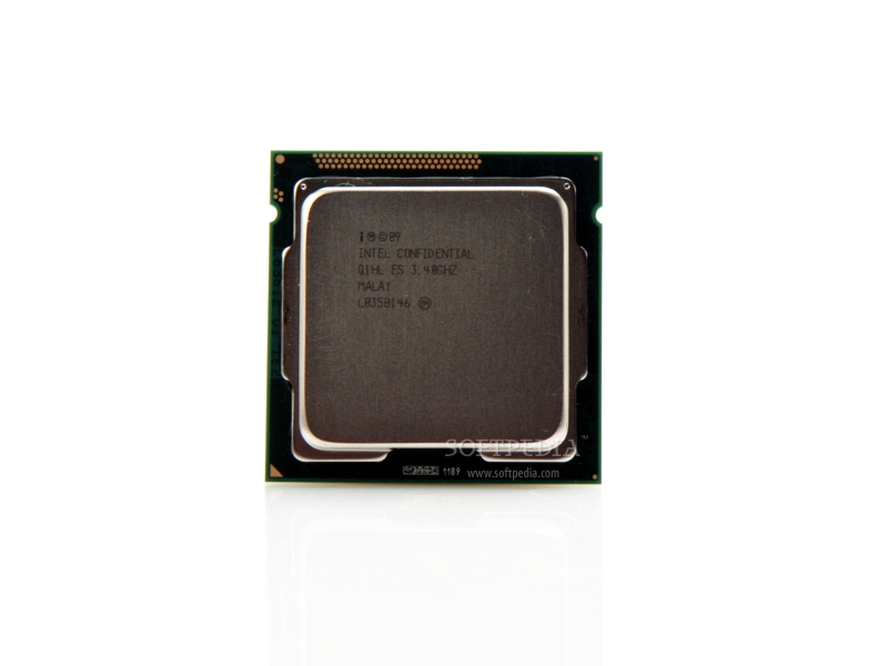
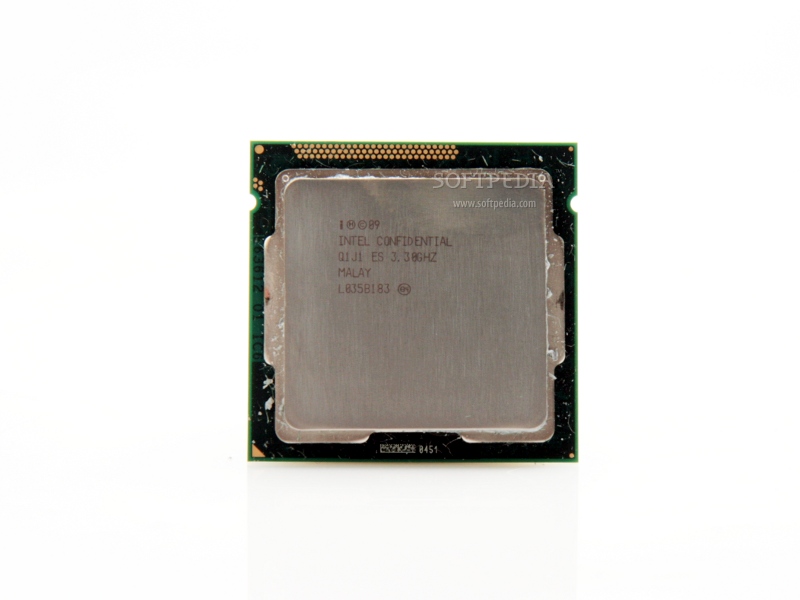
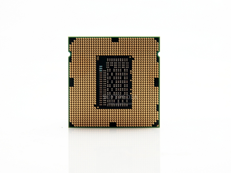
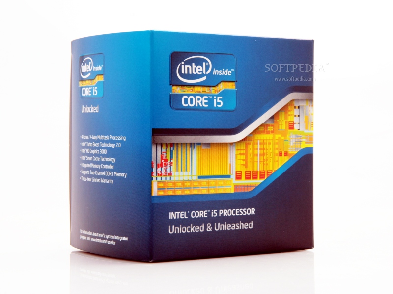
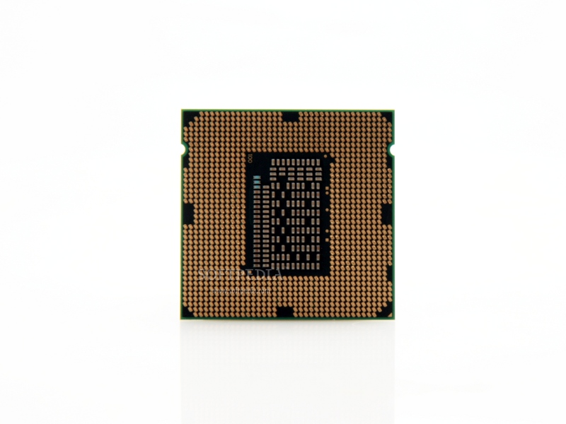
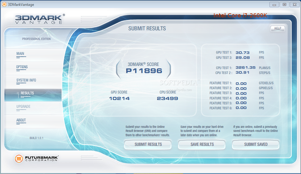
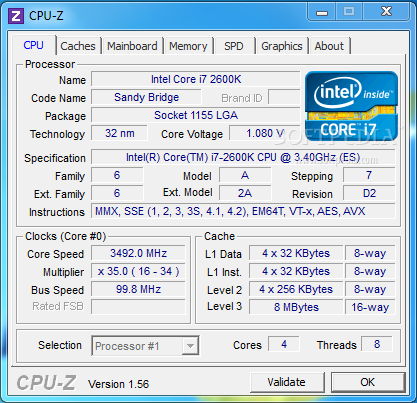
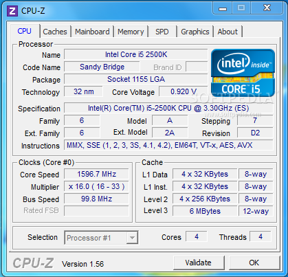
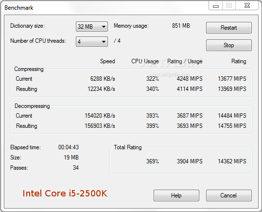
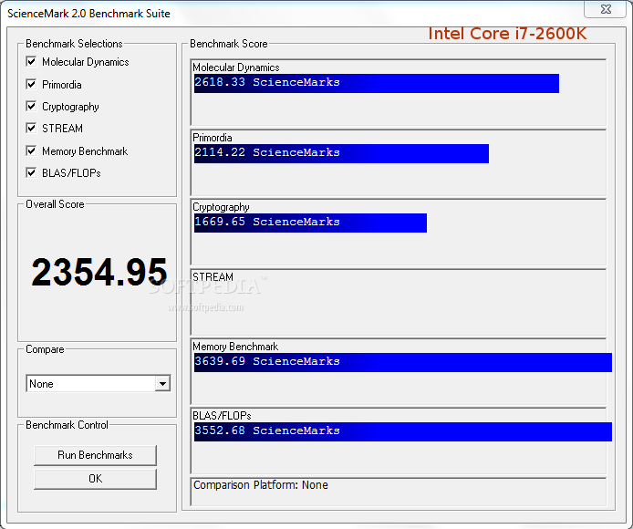
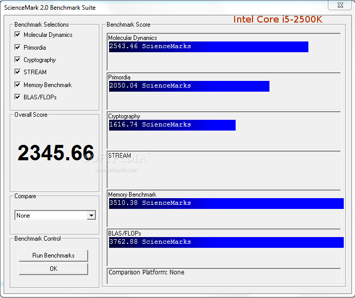
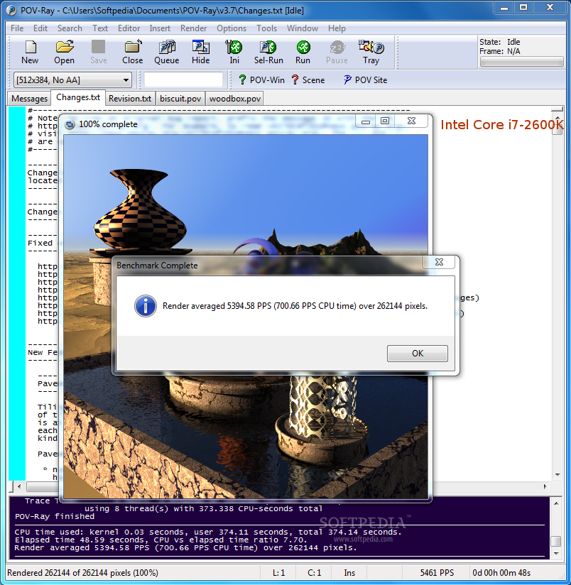
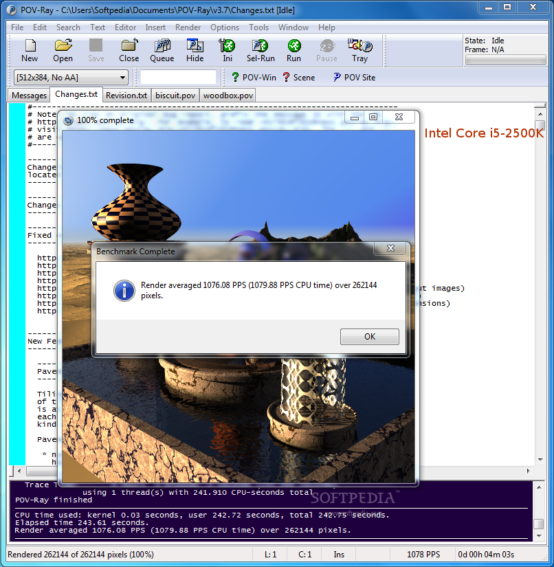
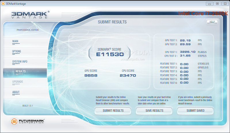
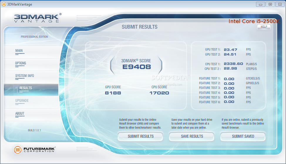
To see what Sandy Bridge is capable of, we had at our disposal two processors, the Core i7 2600K and the Core i5 2500K, both of these shipping with an unlocked multiplier to allow for an increased overclocking potential.
The specs of these two models can be viewed in the first part of the article, but I have also enclosed them bellow for easier comparison.
Intel Core i7-2600K
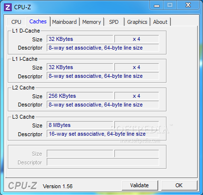
CPU Base frequency: 3.4GHz TDP: 95W Core/ Threads: 4/8 Max Turbo Frequency: 3.8GHz DDR3 Speed: 1333MHz L3 Cache: 8MB Integrated Graphics: Intel HD 3000 Graphics Max Dynamic Frequency: 1350MHz Intel Hyper-Threading technology Intel Advanced Vector Extensions (AVX) Intel Quick Video Sync Intel AES-NI Intel Virtualization technology
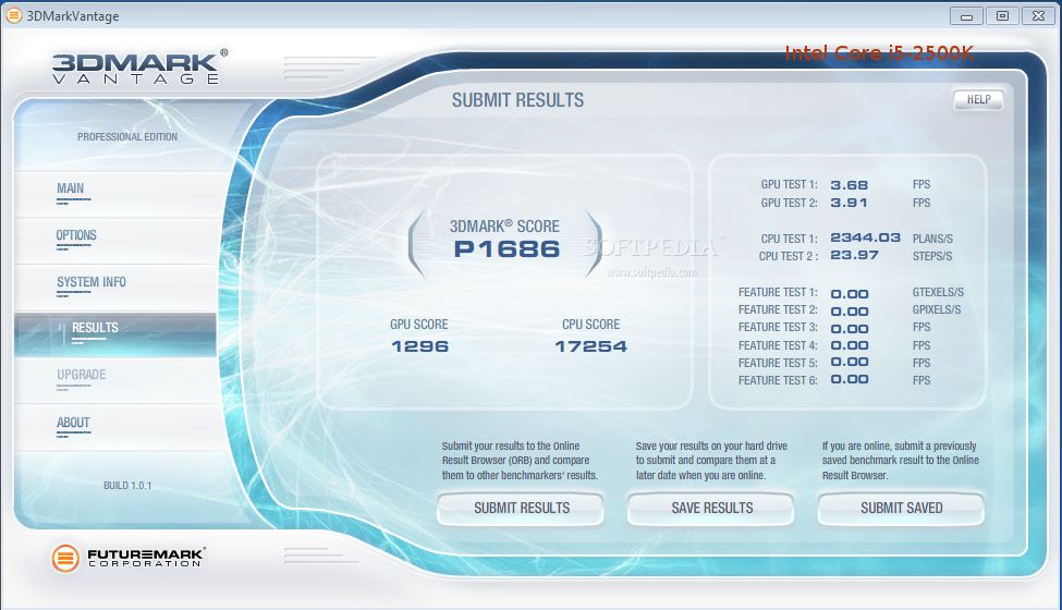
Intel Core i5-2500K
CPU Base frequency: 3.3GHz TDP: 95W Core/ Threads: 4/4 Max Turbo Frequency: 3.7GHz DDR3 Speed: 1333MHz L3 Cache: 6MB Integrated Graphics: Intel HD 3000 Graphics Max Dynamic Frequency: 1100MHz Intel Advanced Vector Extensions (AVX) Intel Quick Video Sync Intel AES-NI Intel Virtualization technology
As you can see from the specs included, these two processors are actually very similar, the major difference between the two being the Intel Hyper-Threading support.
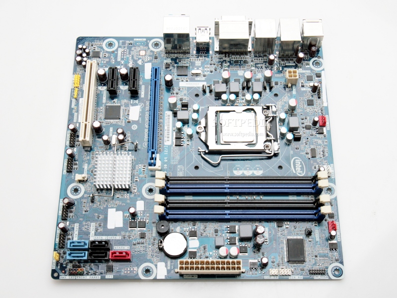
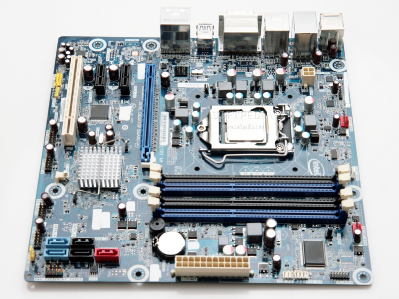
In order to test the CPUs, we used a motherboard built around Intel's P67 chipset, namely the Gigabyte P67A-UD5.
Although a step below the UD7, this board features an advanced design as it uses no less than 20 phases for providing juice to the processor installed.
All the phases are built using DrMOS chips and are cooled via two heatsinks connected together with a black heatpipe that goes along very well with the overall look of the motherboard.
As all other P67 base boards, the P67A-UD5 features four memory slots that can accommodate up to 32GB of DDR3 RAM memory, the boards expandability options being made up of three x16 PCIe slots (one operating at x16, one at x8 while the latter works at x4), a pair of PCIe x1 slots and an regular PCI slot.
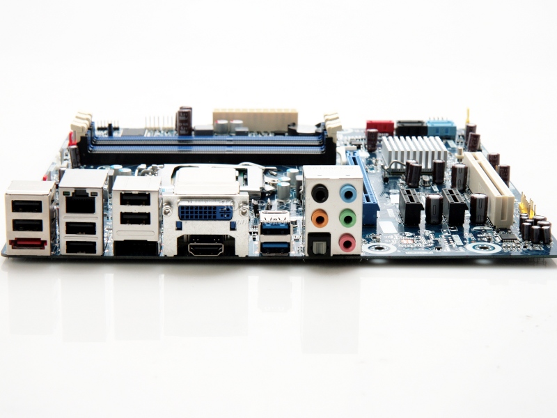
The back panel hosts four USB 3.0 slots, dual USB 2.0/eSATA ports, two FireWire connectors (a regular and a mini-sized one), a Gigabit Ethernet port as well as 7.1 channel sound.
Since the UD5 is an enthusiast motherboard, Gigabyte added on-board Power, Reset and Clear-CMOS buttons, a BIOS debug display sadly missing from the specs list.
To test the integrated graphics we used an Intel DH67BL motherboard that is built around the H67 chipset.
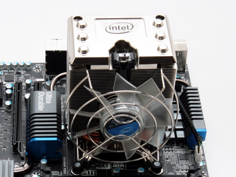
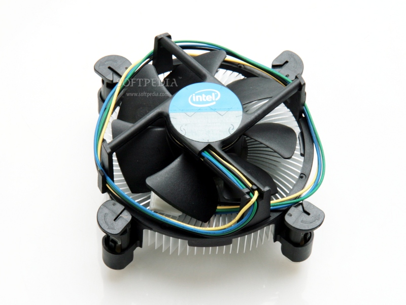
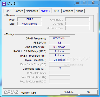
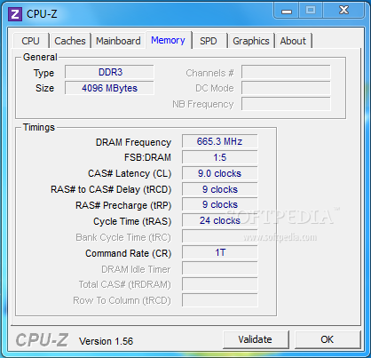
The test system used: Intel Core i7 2600K and Core i5 2500K processors Gigabyte P67A-UD5 motherboard Intel DH67BL motherboard Nvidia GTX 260 216 graphics card Kingston KHX2000C9AD3T1K3/6GX memory kit Kingston SSDNow V+ 64GB Integrated Audio and Network Windows 7 Ultimate 64-bit Operating system Intel LGA 1155 tower cooler
Real-Life Performance
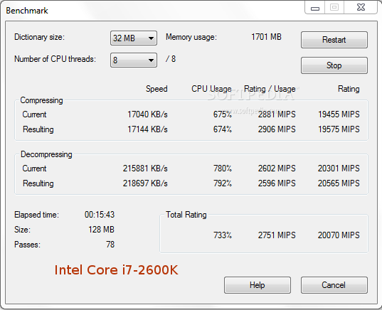
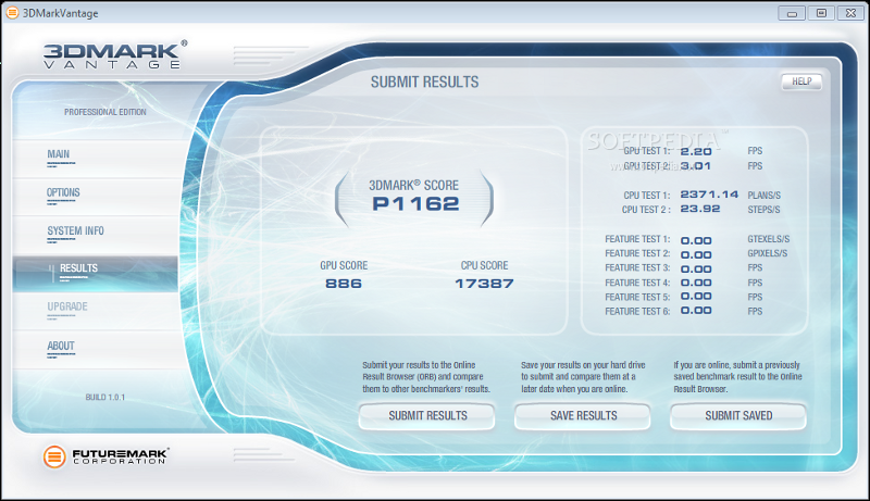
Taking a look at the numbers returned by our benchmark suite reveals that both these new processors are able to deliver top-notch performance for computing enthusiasts.
However, you have to keep in mind the fact that Sandy Bridge wasn't developed in order to take on Intel's Core i7 900 series processors as these will remain the company's top of the line CPUs until the Sandy Bridge E architecture is released.
But this doesn't mean that Sandy Bridge can't deliver an impressive performance.
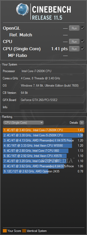
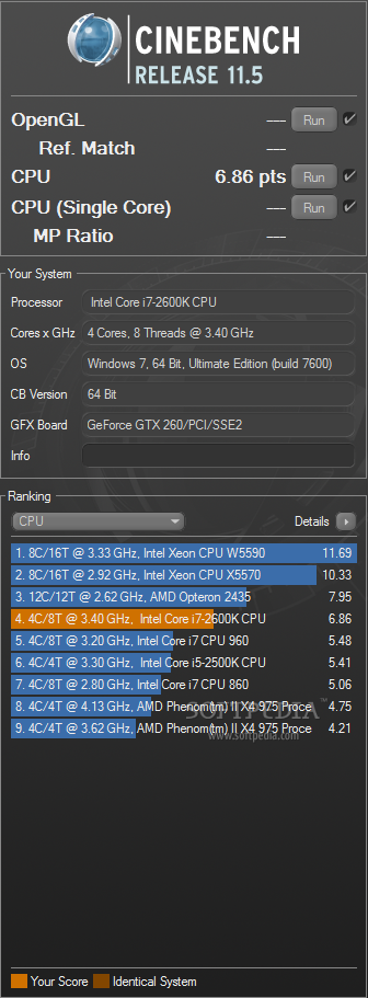
On the contrary, if we take a look at the single-core performance numbers delivered by the CineBench 11 benchmark we would see that the 2600K is about 28% faster than the Bloomfield-based Core i7 960.
You could of course argue that the 960 is lower clocked than the 2600K, but that doesn't change the fact that a 6% speed increase translates to a 28% better result.
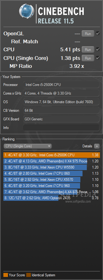
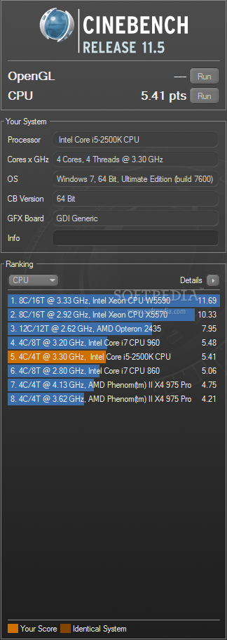
Furthermore, the lower clocked Core i5 2500K performs in a similar manner, even managing to come extremely close to the Core i7 960 in the multi-threaded version of CineBench.
Keep in mind that the 2500K doesn't feature Hyper-Threading support and thus is limited at running only four threads at once, compared to the eight threads the 690 is capable of handling.
As for the difference between the Core i5 2500K and the Core i7 2600K, the results are rather obvious.
The Core i5 can pretty well keep up with its older brother as long as heavy-threaded tasks aren't run as the 100Mhz clock difference between the two isn't enough for the 2600K to take a significant lead.
However, once you start running heavy parallel applications such as video encoding of rendering, the 2500K is no match for the Hyper-Threading enabled 2600K.
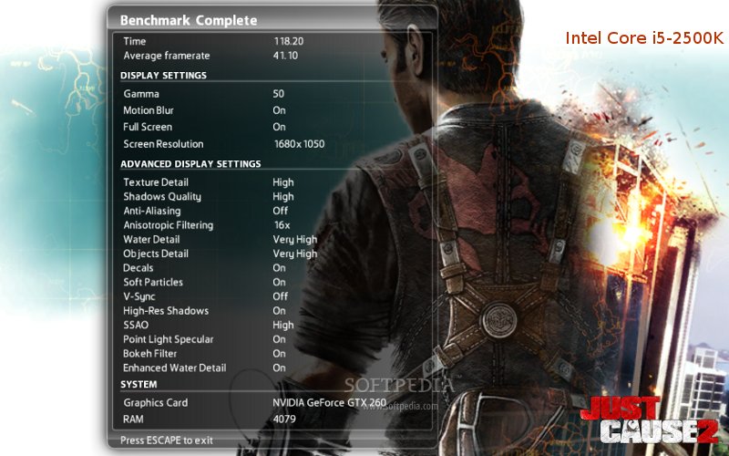
Fortunately, for some of you, games aren't among the software programs that get a boost from having more cores, a better graphics card being a far better investment than a 2600K at this point.
Integrated graphics performance
In the computing power of the new Sandy Bridge CPUs is nothing to blow us away, the same thing can't be said about its integrated graphics as Intel has made great strides in this direction with its new architecture.
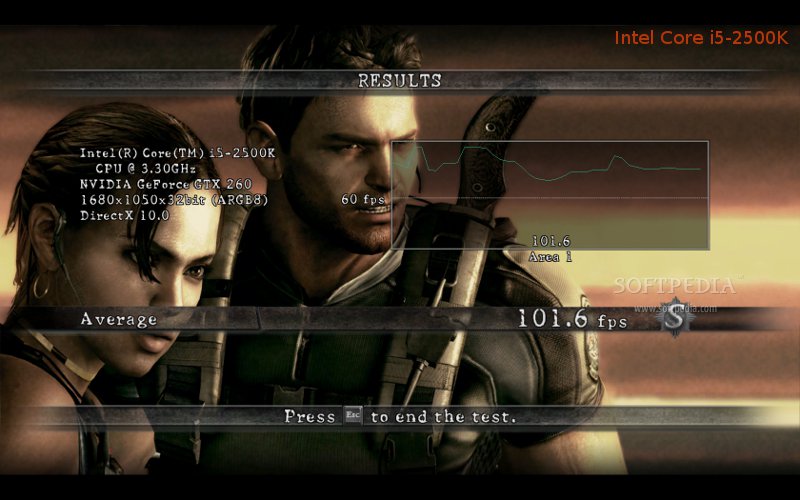
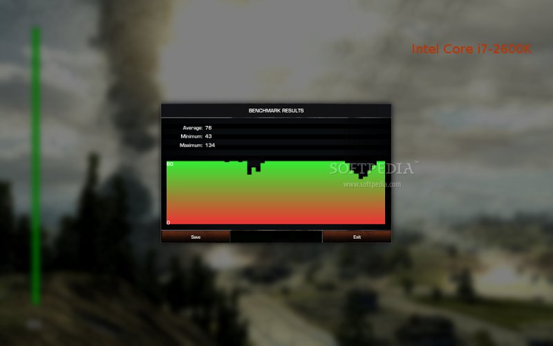
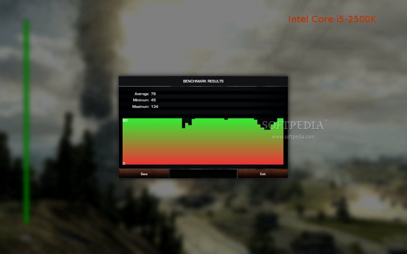
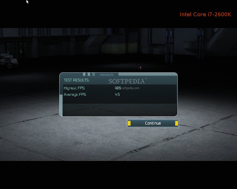
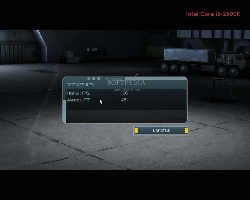
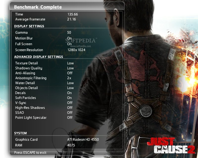
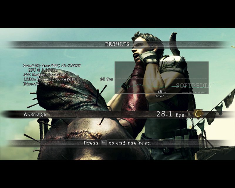
Taking a look at the numbers provided, one can clearly see that the new Intel HD 3000 graphics are able to deliver some nice results, two of the three games tested being completely playable, with frame rate above 30fps.
Of course, users will be limited to resolution such as 1280x1024, but this is completely acceptable for an integrated solution.
In addition, the graphics frequency difference between the 2600K and the 2500K won't make for an impressive performance increase, a good new for laptop owners as mobile CPUs have the integrated graphics clocked at lower speeds than their desktop counterparts.
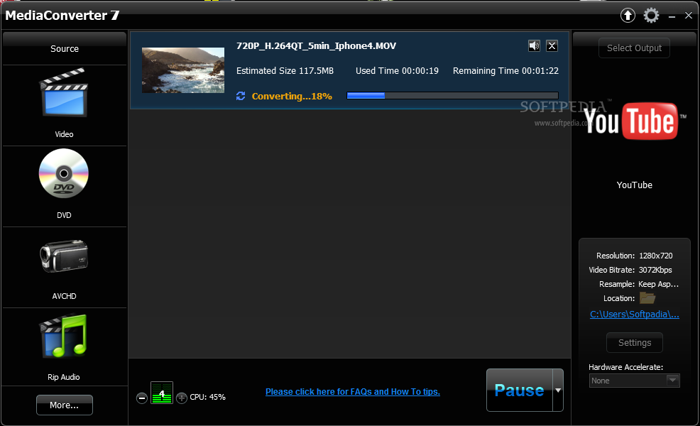
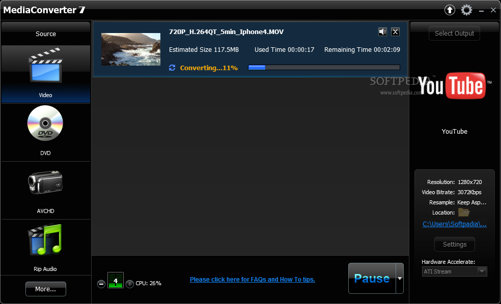
As stated earlier, together with the new GPUs, Sandy Bridge processors have also released a media engine that adds hardware video encoding support, a treat that was reserved for dedicated graphics cards in the past.
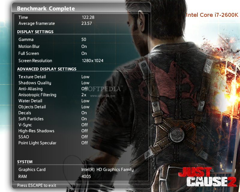
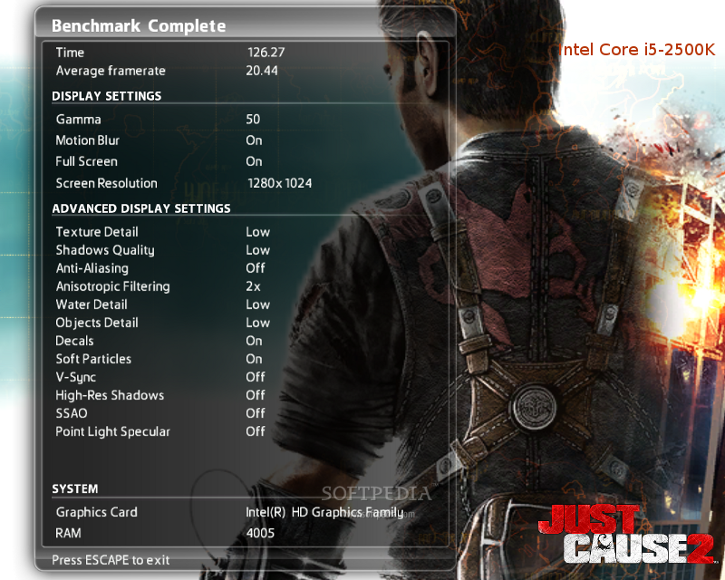
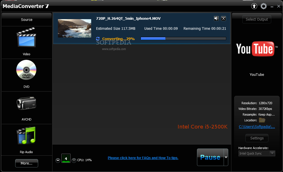
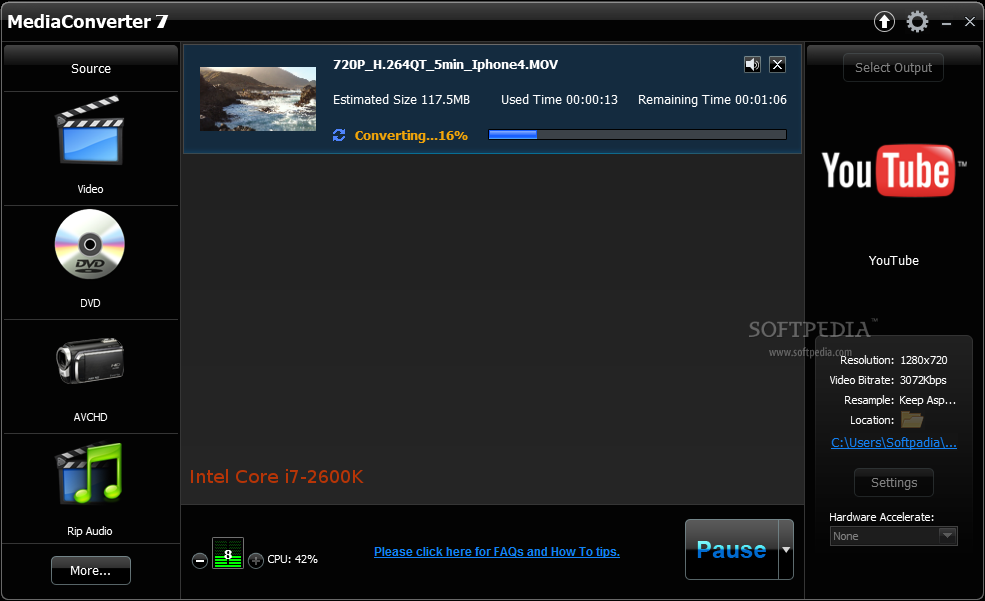
To test this, we used ArcSoft's Media Encoder 7 application (one of the few software encoding solutions available to support Intel's QuickSync technology) for encoding a 10Mbps, 720p resolution H.264 MOV video file to a 3Mbps MP4 file.
As you can certainly see, the QuickSync technology managed to cut the time needed for this task from 101 seconds to 30 seconds when using an Intel Core i5 2500K processor.
In the case of the Core i7 2600K CPU, the total time required went down from 99 seconds, when using the CPU alone, to 28 seconds with QuickSync activated.
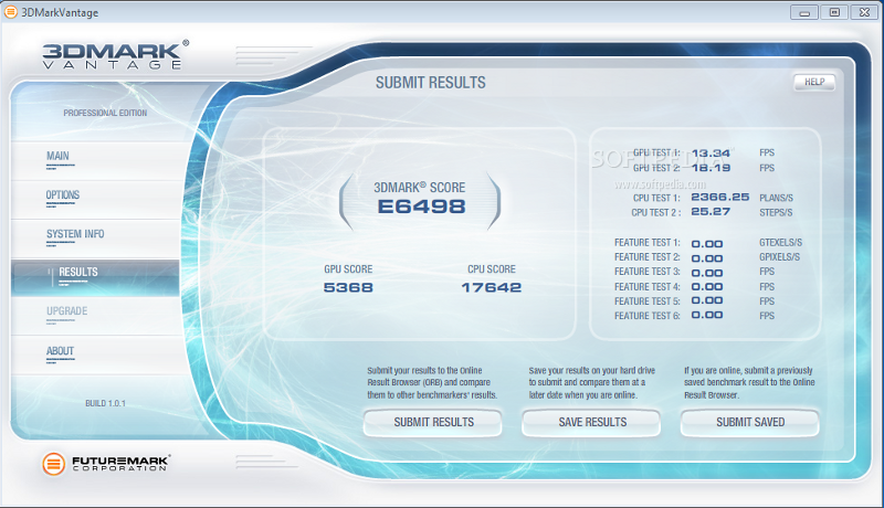
To put things in perspective, I have also included the results of a Radeon HD 4550 graphics card.
Although the 4550 is a stand-alone card, the Intel HD 3000 integrated graphics manages to beat its hands down in every game run and even in the media encoding test.
However, it does so in a way much different than before, since the most important highlight about Sandy Bridge is not its processing power but the new integrated graphics. Don't get me wrong, the computing performance is certainly there as Sandy Bridge has the muscle to take on Bloomfield in some applications, but its GPU is a lot more interesting, especially when you consider its media encoding capabilities. What this basically means is that Intel is now capable of delivering integrated graphics that are on par with some entry-level graphics cards, and, although that doesn't sound like much in the desktop space, mobile computers will most certainly feel the difference. In addition, the chips new media encoding capabilities can dramatically shorten the time required for encoding video files and, knowing Intel, support for their CPUs will become widely available in software applications everywhere. And this leads me to another technology that Intel introduced in Sandy Bridge. I am talking about AVX, the new instructions that should improve SIMD processing speed. Although not very popular right now, this will most certainly make a strong showing in the near future, further improving Sandy Bridge's performance in highly parallel applications such as graphics rendering. This, will in turn, make Sandy Bridge more powerful when compared with Nehalem CPUs in the future, although nobody, at this point, can tell us how much we'll have to wait until this happens. And then there's the price. When it set Sandy Bridge out to market, the Santa Clara-based company went with a pretty aggressive price strategy when compared to Westmere and older Lynnfield processors as the same amount of money can get you a higher core count or a faster clocked SKU. However, the good news ends here, as Intel has also made some strange decisions when it designed Sandy Bridge such as the artificially limited overclocking potential. Although a wide range of explanations about why this happened was available from Intel, the truth of the matter is that Sandy Bridge actually fell victim to its own success as the Santa Clara company had to do something not to cannibalize its Core i7 900 series processors until Sandy Bridge E arrives. And the solution was to limit the overclocking potential of their chips. Fortunately, this doesn't change the fact that Sandy Bridge is one of the best overclocking chips available right now (if you choose a K series processor that is) as you will see in a follow up article detailing our overclocking tests. Finally, as everyone expected it to, Sandy Bridge proves to be a success, Intel managing to bring Nehalem-like performance to a more than attractive price point with powerful integrated graphics to boot. The Good:
- Strong performance
- Integrated graphics
- Hardware video encoding acceleration
- Competitive price
- AVX instruction set
- Turbo Boost 2.0 The Bad:
- Artificially limited overclocking potential
- Requires new LGA 1155 motherboards.Conclusions