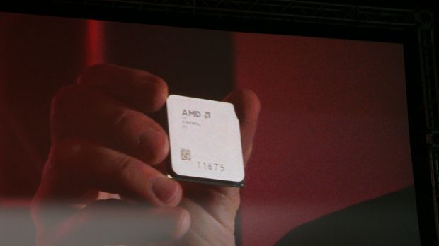
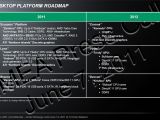
Expected to arrive in 2012 as the successor of the recently launched Llano chips, AMD's Trinity accelerated processing units will use a new socket that goes by the name of FMX and appears to be incompatible with both the current FM1 and AM3+ packagings.
Little is known about this socket at present, outside of the fact that motherboards that will include it still support DDR3 memory, but AMD just confirmed that it will be used for both Trinity and the upcoming Komodo APUs.
Expected to arrive in 2012, Trinity will be AMD's first accelerated processing unit to use the high-performance Bulldozer architecture and will include one or two such modules to form dual and quad-core chips.
The x86 processing cores will be paired together with a Radeon HD 6000-series integrated graphics core, which uses a VLIW4 arrangement.
The rest of the chip die will be occupied by 8MB of Level 2 cache as well as by an integrated memory controller and other similar ICs and the whole Trinity chip is expected to feature more than 2 billion transistors.
As it's the case with the current Llano APUs, Trinity won't feature any sort of Level 3 cache memory, as AMD wanted to save the die space for the integrated GPU.
Earlier today, AMD has released its first high-performance APUs which are based on the Llano architecture and target the mainstream notebook space.
The initial launch includes seven mobile processors (an additional E-Series APU is expected to arrive a bit later) that feature between two and four processing cores and have a TDP of 35 or 45 Watts, depending on the model.
Outside of the x86 CPU cores, Llano APUs also include a Radeon HD 6000-derived graphics core that packs between 160 and 400 stream processors, which work at either 400MHz or 444MHz. (via Sweclockers)

 14 DAY TRIAL //
