14 DAY TRIAL //
 United Microelectronics Corp. announced that it is successfully preparing its first 14nm FinFET tech for tape-outs together with ARM, that should be ready this year.
To prove this point, UMC and ARM recently finished taping out a process qualification vehicle (PQV) that will be the testbed for the upcoming 14nm finFET tape-outs. Yes, before taping out a new semiconductor technology, a testbed for it must be tested too. The test chip is designed to validate ARM Cortex-A family core on a new fabrication process.
UMC and ARM clients will be able to license these new physical building blocks from ARM and basically build them into their designs at UMC.
Together with the 14nm FinFET tape-outs, the IP enablement process will begin for the rest of the ecosystem needed for UMC's FinFET tech that includes a new ARM processor physical design.
For those who don't know, tape-outs are the last technical tests of a prototype technology before entering production, usually this signifying that a launch date will become available in the near future.
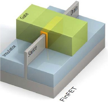
A short FinFET presentation
FinFET technology is a rather new technology in the semiconductor fabrication industry. Replacing the Mosfet semiconductors, it places a silicon fin through the gate electrode while containing the source and drain elements of the silicon fin outside and around the gate instead of underneath it. This way reducing the gate electrode size for overall transistor size reasons, the current will not have to pass through an n-well anymore but through the silicon fin that crosses the gate electrode.
FinFET technology is, however, extremely expensive to manufacture, and although it offers higher transistor performance, it's still a manufacturing conundrum at the moment over the classical Mosfet.
UMC probably wants to impress its much more experienced partner ARM, together with all possible clients of its manufacturing prowess. Keeping in mind that Skylake will also come with a 14nm die size, Intel will probably look at the tape outs with interest.
UMC expects its 14nm FinFET testing process to be finished by late 2015 and ready for customers shortly after.