Present at IDF 2015, Samsung has confirmed that it will start producing HBM (High Bandwidth Memory) technology as well, removing the HBM exclusivity from the, until now, stacked memory manufacturing leader SK Hynix.
Being a NAND flash memory worldwide leader, Samsung sees the great potential HBM tech has in the foreseeable future and decided to invest in developing products that will feature the advanced stacked memory technology. However, Samsung decided to start manufacturing only second-generation HBM2 technology, since the first generation present on AMD’s R9 Radeon Fury series is considered not to have the desired densities and clock-rates.
In addition, Samsung believes that HBM technology will have many useful applications in high-performance GPUs of the future and believes that incredible capacities and bandwidth speeds will be achieved via six HBM devices on GPU dies.
Although professional graphics cards like AMD FirePro series and NVIDIA’s Quadros still use GDDR5 memories because of their aboveaverage memory sizes and reliability, this is believed to change next year when HBM technology reaches maturity and is able to provide enough storage and bandwidth to satisfy professional designers and 3D graphics artists with high-performance computing using GPU-based solutions.
HBM2 bandwidth speeds could reach 6144-bit
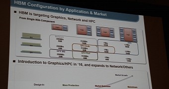
Right now, Samsung works at delivering multiple HBM stacked memory packages featuring two, four or even eight 8Gb stacked memory modules on a base die with 1024-bit interface. According to slides offered by ComputerBase.de, the max data rates of Samsung’s HBM eight stacked memory modules can reach 2Gb/s, which will give up to 256GB/s of bandwidth per chip.
Samsung believes that this way it will be able to target different market segments with new GPUs, APUs, and will be able to develop a high variety of applications by introducing the right amount of HBM controllers into their chips.
Since graphics cards are the first to use such technology, it’s very much possible that a mid-entry GPU die could hold a two-package (2Hi ) HBM device with a 2GB frame-buffer with 256GB/s bandwidth, while the more advanced GPUs will hold six HBM stacks allowing 1TB/s bandwidth, enabling cards to reach incredible on board memory sizes of 12GB, 24GB or 48GB.
This sort of projects isn’t, however, unknown to manufacturers like AMD and NVIDIA who both prepare graphical solutions in 2016 that are based on HBM2 technology. AMD’s “Arctic Islands” architecture and NVIDIA’s “Pascal” are both targeting 32GB of onboard memory for their future products. Although it’s known that both AMD and NVIDIA work on 14/16nm FinFET process technology, it’s unknown what sort of process technology Samsung will use for its HBM2 next-gen memory devices.

 14 DAY TRIAL //