Intel fully decided to unwrap all the Skylake details during its IDF 2015 conference in San Francisco.
The new 6th generation CPU from the American giant swept the market this August at Gamescom, when it was announced together with the new Z170 chipset. Intel kicked off right from the start with two models built for enthusiasts, the Core i7-6700K and Core i5-6600K.
After many reviews of the new CPU models hit the press, including our own Core i7-6700K review, more official details were awaited by enthusiasts about the innards of the new Skylake architecture. During IDF 2015 Intel delivered what the public was expecting.
Intel's latest System-on-Chip or SoC microarchitecture brings better performance, better design and new IPs on a 14nm process manufacturing that surpasses anything currently being available from the competition in both performance and chip density.
Where it began, and how it ended to be
The story of Skylake started with plans from Intel just to build a 3x TDP scale, 2x form factor range and a classic set of PC IO after multiple iterations and test versions the eventual SoC became bigger, wider and ended up with a 20x TDP scale, 4x form factor range, offering multiplatform I/O features from PCs to tablets that will be available in late 2015.
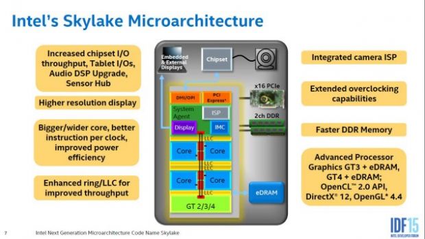
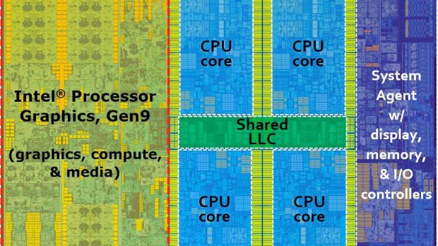
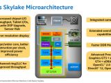
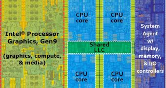
The core block of a Skylake chip includes four cores that share an LLC through an interconnect ring, called SOC ring. On the die there are placed the GT1, GT2, GT3 GPUs, and the more advanced GT3e and GT4e with integrated DRAM that support OpenCL 2.0, DirectX 12 and OpenGL 4.4. Also placed on the SoC chip are the dual channel DDR4 memory controller, the display system for displays both embedded and external, the audio DSPs and sensor hubs with a single integrated camera ISP can be found on the die for better imaging quality.
Corewise, there are vast improvements on the performance given by Skylake since it has improved queues per thread in Hyper Threading than the Haswell: 64 compared to 56 on the Haswell and 28 for Sandy Bridge, while the interconnecting ring that surrounds the cores double the bandwidth without any power being sacrificed. The bandwidth dedicated to loading and storing data is also larger with prefetcher improvements, deeper store buffer, better L2 cache miss bandwidth, improved page miss handling and new instructions for better cache management.
Better, more flexible with a powerful single-thread performance
Overclocking-wise, the Skylake gets a Full Range BCLK improvements and Finer Grain Tuning for DDR4 memory. Giving the Skylake a fully unlocked turbo design that is controllable through dedicated software and BIOS, the full BCLK overclocking allows full range increments over previous Haswell models of 83 in 100 MHz increments, while DDR4 overclocking will also allow smoother and finer increments overclocking increments than the previous generation. To add even more overclocking freedom, even the graphics clock can be tuned with ratios of up to 60 in 50 MHz increments.
However, Intel has dismissed rumors of Inverse Hyper Threading being present on the Skylake die, something that we talked previously as being a cutting edge methodology of single-thread computing boosting via multi-core help. We expected an answer on this matter at IDF and Intel unfortunately dismisses it as being false. Recent studies made by Heise.de showed incredible single-thread computing performance by the new Core i7-6700K and speculated that Inverse Hyper Threading might be present on the new Skylakes. Apparently, it was not.
However, Intel did not explain how such incredible results have been reached by independent testers, since single-thread computing results were double compared to the previous Haswells, while multi-core computations were only marginally better. Even if Intel won't give us more details yet, all Skylake secrets will certainly be unveiled in time.
 14 DAY TRIAL //